PCB assembly and welding technology transforms bare printed circuit boards (PCBs) into fully functional electronic prototypes. The PCB assembly (PCBA) stage combines four core operations: component placement, soldering, quality inspection, and final electrical testing. Manufacturers choose manual or automated workflows for each step, based on production scale and design complexity.
PCB design starts with a schematic diagram. Engineers create a PCB layout from this schematic, which defines electrical connection paths (called wiring) and component placement. Once the layout is approved, fabrication begins. The finished PCB is a rigid sheet of glass fiber bonded with epoxy resin, with copper traces forming the circuit pathways. Components attach to the PCB via soldering—using a metal alloy called solder to fix parts to designated pads. The completed, soldered board is known as an assembled PCB (PCBA), which then undergoes functional testing to validate performance.
1. Core PCBA Mounting Technologies
Three primary technologies power the PCBA process, each suited to different component types and design needs:
(1) Through-Hole Technology (THT) PCBA Process
Through-hole technology (THT) uses components with pins or leads. Engineers insert these leads through pre-drilled holes or pads on the PCB, then solder them to the opposite side of the board. This method creates strong, reliable connections, ideal for larger, high-power components.
(2) Surface Mount Technology (SMT) PCBA Process
PCBs use two pad types: through-hole and surface mount. For surface mount pads, engineers solder surface mount devices (SMDs) directly to the board’s surface. The soldering surface doubles as the component placement area, with solder paste acting as the bonding agent. SMT enables smaller, denser circuit designs, making it the dominant choice for modern electronics.
(3) Hybrid Technology PCBA Process
As circuit designs grow more complex, engineers often combine both through-hole and surface mount components. These mixed-technology PCBs use the hybrid PCBA process, blending THT and SMT workflows to balance performance, size, and reliability.
2. Step-by-Step PCB Assembly Process
The PCBA process order varies by mounting technology, but conventional PCB assembly follows these seven key steps:
(1) Solder Paste Application
First, technicians apply solder paste—a mixture of tiny solder particles and flux—to the PCB’s pad areas. Most manufacturers use stencils (custom-cut to match component pad sizes) to ensure precise, consistent solder paste deposition only on required locations.
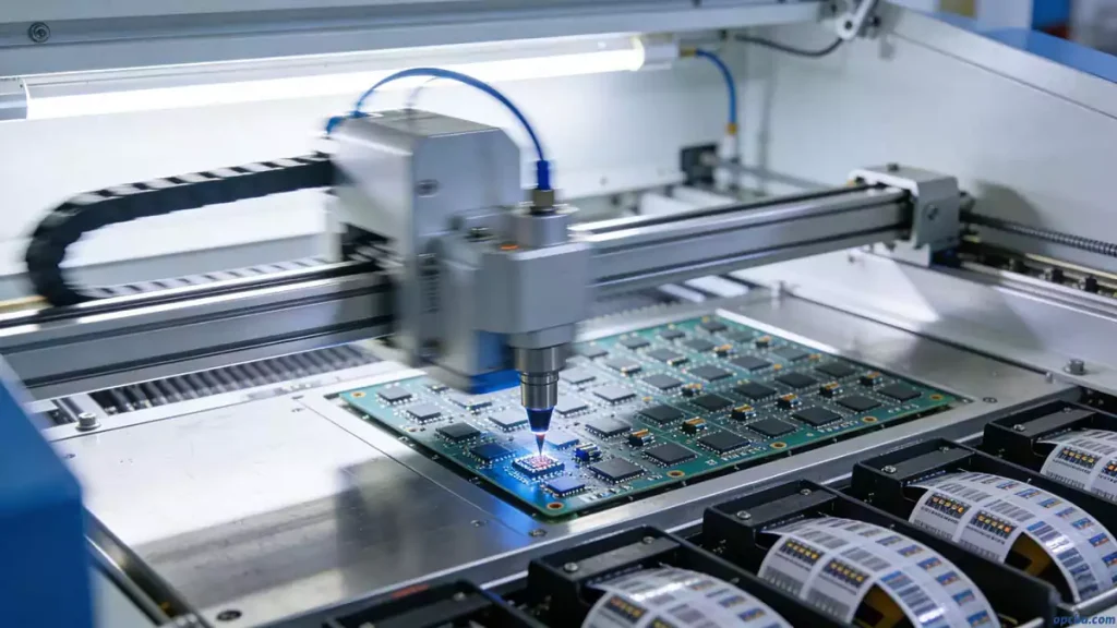
(2) Component Placement
Modern PCB assembly automates this stage with robotic pick-and-place machines. In the past, engineers manually placed components like SMDs; today, these machines accurately position parts on pre-planned PCB areas, reducing human error and boosting speed.
(3) Reflow Soldering
With solder paste and components in place, the board moves through a reflow oven. The oven’s heaters melt the solder in the paste, bonding components to the PCB pads. After melting, the board travels through cooler zones to solidify the solder, creating permanent, reliable electrical connections.
(4) Post-Reflow Inspection
After reflow, technicians inspect the PCB to catch defects like poor solder joints, misplaced components, or short circuits. Manufacturers use multiple inspection methods: manual visual checks, automated optical inspection (AOI), and X-ray inspection (for hidden joints). Faulty boards are either reworked (for minor issues) or scrapped (for critical failures).
(5) Through-Hole Component Insertion
Some PCBs require both SMD and through-hole components. This step focuses on inserting through-hole parts, which use plated through holes (PTHs) to connect signals across the board. Technicians insert components manually or use wave soldering for automated assembly.
(6) Final Functional Testing
Engineers perform a second, comprehensive inspection to validate the PCBA’s electrical performance. This includes testing voltage, current, and signal output to ensure the board meets design specifications. Advanced testing equipment helps manufacturers confirm whether the finished board functions as intended.
(7) Cleaning & Preparation
Soldering leaves flux residue on the PCB, which can degrade performance over time. Technicians clean the board with deionized water to remove residues, then dry it thoroughly with compressed air. The cleaned PCBA is now ready for customer delivery and final inspection.
3. Key Welding Techniques in PCBA
All PCBA processes rely on soldering (welding) to connect components to PCBs. Five common soldering techniques serve different application needs:
(1) Wave Soldering
Wave soldering is the most widely used method for THT and hybrid PCBA. The PCB moves over a flowing wave of molten hot solder, which solidifies to form strong, permanent component bonds. Learn more about lead-free SMT reflow and wave soldering best practices in our guide: SMT Reflow & Wave Soldering for Lead-Free PCBA.
(2) Brazing
Brazing uses high temperatures to create the strongest welds. It heats metal components to join them, melting a filler metal to bond the base materials. This technique is ideal for heavy-duty, high-stress applications.
(3) Reflow Soldering
Reflow soldering uses heated solder paste to attach SMDs to PCBs. The molten solder connects component pins to PCB pads, creating reliable, low-resistance connections—this is the core method for SMT assembly.
(4) Soft Soldering
Soft soldering is perfect for small, delicate components. It uses a tin-lead alloy filler metal, heated with an electric soldering gun or gas torch, to bond parts to the PCB without damaging fragile components.
(5) Hard Soldering
Hard soldering creates stronger bonds than soft soldering, using temperatures around 600°F (315°C) to join metals like copper, brass, silver, or gold. It suits applications requiring durable, high-temperature-resistant connections.
4. DFM: Ensuring Smooth PCB Assembly & Welding
Design for Manufacturing (DFM) errors in PCB design can force engineers to revisit the layout stage, causing costly delays and wasted resources. Multiple iterations of this cycle waste time, money, and manpower. A robust DFM strategy streamlines the entire design-to-assembly process, minimizes unexpected issues, and ensures predictable production costs.
opcba provides reliable PCB assembly services in China, covering all stages of PCBA and welding technology. Whether you need THT, SMT, or hybrid assembly, our team delivers high-quality, cost-effective solutions. Learn more about our end-to-end one-stop PCB assembly solutions in our guide: What is the One Stop PCB Assembly Services? Contact us today to discuss your PCB assembly project.


