A PCBA solution isn’t just a stack of Gerber files and a BOM. It’s the design, the sourcing, the assembly, and the debugging that turn a block diagram into a box of working boards. Over the years, I’ve seen how easily a small oversight in early planning can cascade into a line-down situation during production. This guide unpacks the stages, the gotchas, and the way we approach it at OPCBA.
What a PCBA Solution Actually Covers
When someone talks about PCBA solutions, they mean the full chain: understanding what the product does, selecting the right components, laying out the board, fabricating it, populating it, and verifying the result. The goal is a board that passes functional test on the first pass—not the third.
Where the Development Process Starts (And Often Stumbles)
Before a single component is placed, we sit down with the customer and define the real requirements. That means more than just a schematic. It means asking about operating temperatures, regulatory standards, whether the product will live outdoors or in an air-conditioned lab. I once had a project where the design assumed a constant 25°C environment; the first prototype shut down at 60°C in the field because no one had talked about the enclosure. That conversation saves months.
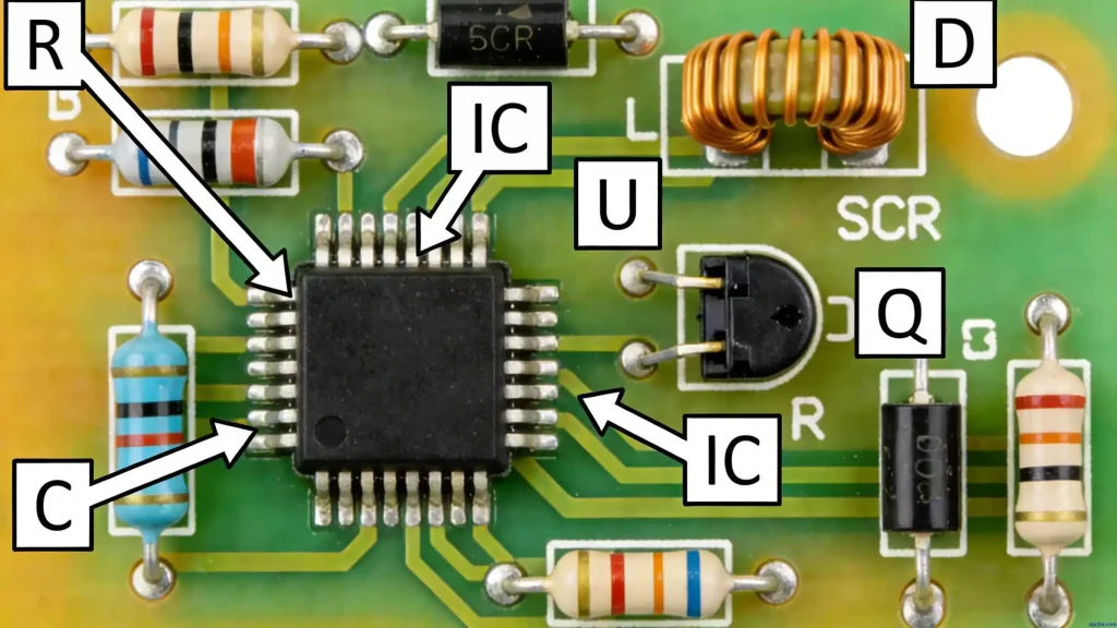
Once the requirements are solid, the principle design phase picks the core chips and maps out the functional blocks. Here, a PCBA solution development team looks beyond the datasheet to supply chain reality. Is that microcontroller available in volume? Is the footprint compatible with a second source? These questions shape what gets drawn.
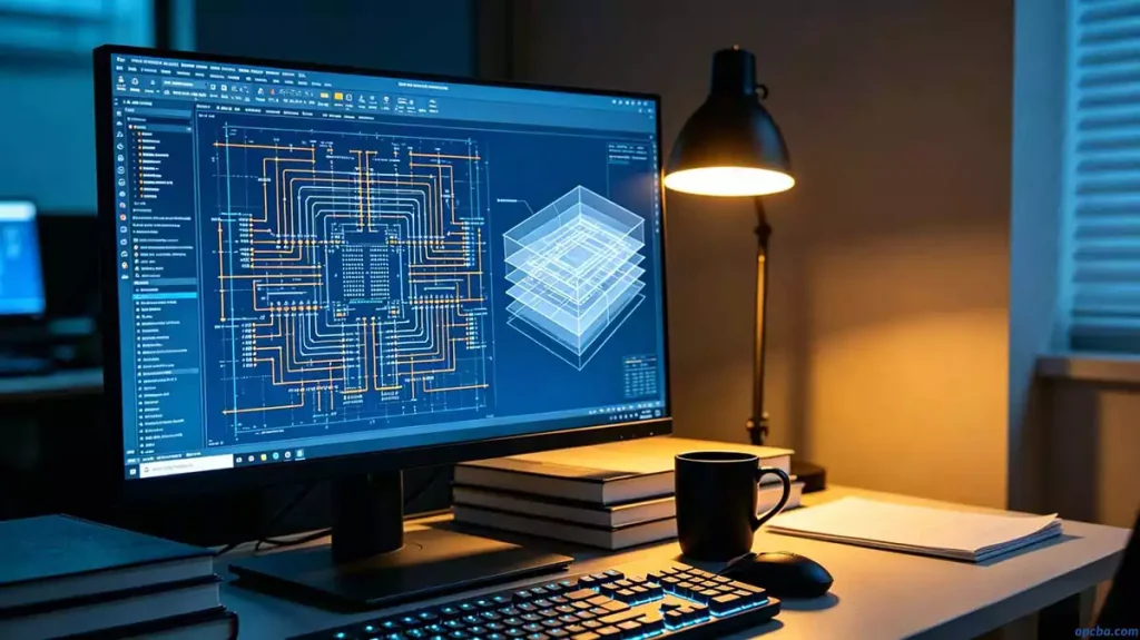
Then comes PCB layout. This is where signal integrity, thermal paths, and electromagnetic compatibility become real. We determine stackup, trace widths, layer counts, and copper weights based on the mechanical constraints and the electrical demands. I’ve learned that rushing into routing without a rigorous stackup review creates impedance mismatches that are a nightmare to debug later.
If you want to dig deeper into the layout rules and techniques that make a board manufacturable and reliable, our PCB Design guide walks through the practical steps and decisions involved.
Component Sourcing: The Unseen Half of the Battle
The most beautifully laid-out board means nothing if the parts can’t be procured. Our PCBA solution development team works closely with suppliers to lock in lead times, verify authenticity, and cross-check specifications. We’ve pulled the plug on a design at the review stage because a key connector was marked “end-of-life” six months prior. Catching that early avoided a costly redesign.
From Bare Board to Assembly Line
PCBA assembly uses SMT and sometimes through-hole processes depending on the mix. The boards go through solder paste printing, automated pick-and-place, reflow, and then inspection. For mixed-technology boards, the DIP section follows. I’m a firm believer in first-article inspection and SPI data trending—without that, a single clogged stencil aperture can create hundreds of open joints before anyone notices.
Testing: The Stage Where “Working” Is Verified
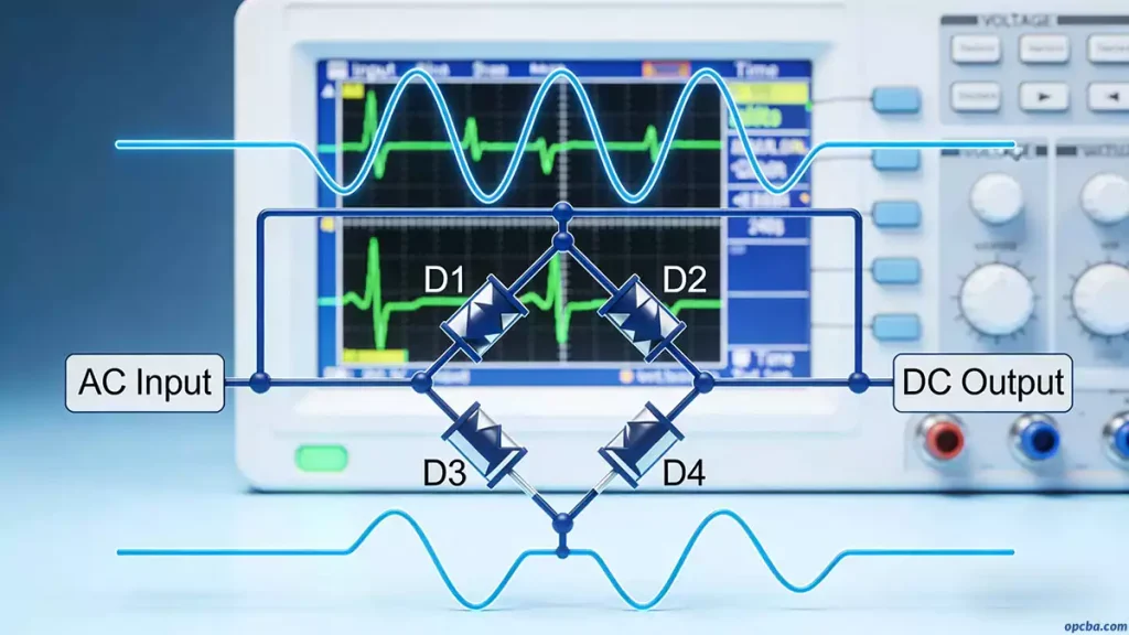
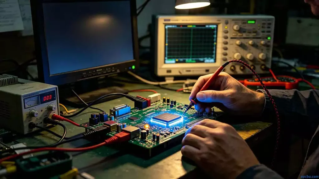
After assembly, every board undergoes functional testing. This isn’t just a power-on check. We verify voltage rails, signal outputs, and key waveforms against the specification. Thermal imaging under load often reveals hotspots that simulation missed. From there, debugging and optimization tighten the performance margins. I’ve seen a simple ferrite bead placement change reduce radiated emissions by 10 dB, turning a marginal EMC test into a clean pass.
The Team and Tools Behind Reliable PCBA
A solid PCBA solution needs an interdisciplinary team—electronic engineers who understand analog and digital design, layout specialists who know DFM, and process engineers who run the SMT line. Tools matter too: precise solder paste inspection and automated optical inspection aren’t luxuries; they’re standard equipment for repeatable quality. Supply chain management ties it all together, ensuring components arrive on time and pass incoming inspection.
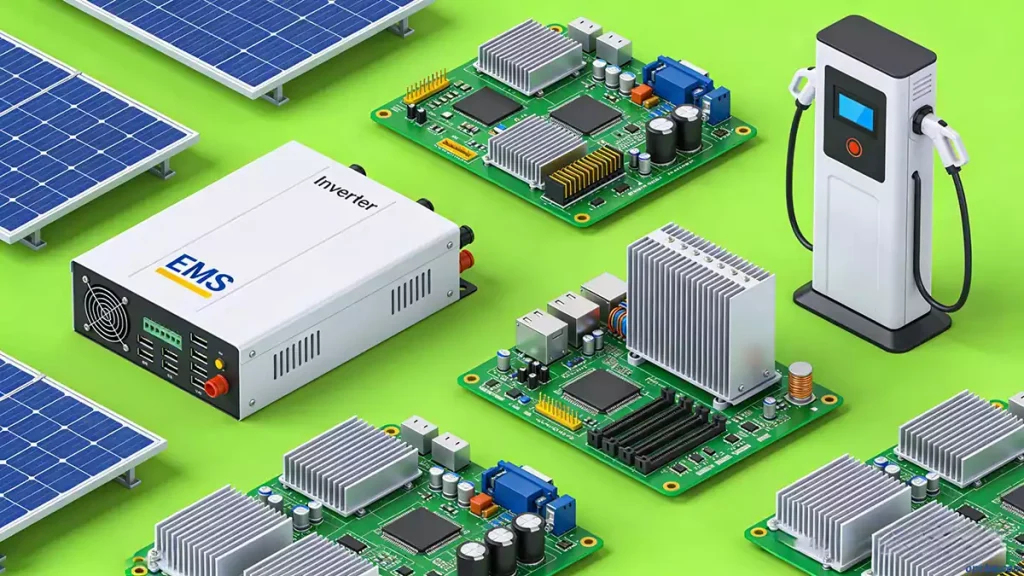
OPCBA’s one-stop service covers this entire spectrum, from initial PCBA solutions development to mass production. If you’re not sure how a one-stop model differs from managing multiple vendors separately, our guide on What is the One Stop PCB Assembly Services? explains the key advantages and what to look for.
Our experience spans telecom, automotive electronics, industrial control, and home appliances. If you have a product concept and need a partner to handle the board-level design and assembly, reach out—we’ll talk through your requirements and map out a plan that fits.