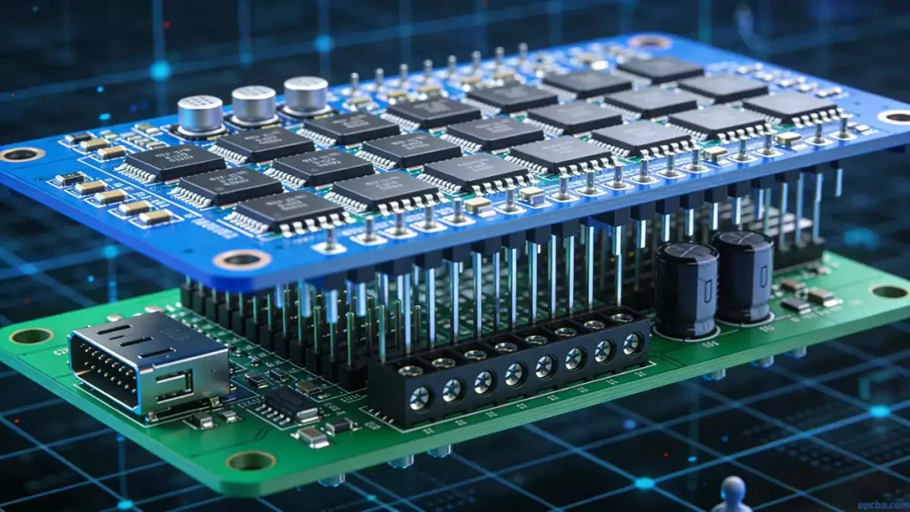
Robot PCBA is the core electronic control unit for robotic automation systems. It powers the brain of Industrial Control, collaborative, and service robots, enabling precise control, motion feedback, and stable operation. As robotic adoption grows across industries, compliant, high-reliability robot PCBA solutions have become critical for automation equipment manufacturers.
Robot PCBA forms the robot’s core control system — one of the five key components that ensure robotic operation. The other core robot components include sensors, motion and feedback modules, the robot body, and the power supply. Since this control assembly directly governs a robot’s performance and safety, manufacturers can never compromise on its design, structure, and manufacturing quality.

1. Critical Design Considerations for Robotic PCB Assembly
Robotic circuit board processing starts with schematic design. This phase defines the board’s component layout, electrical performance, and manufacturability. A precise, standardized PCB design avoids costly rework during evaluation and mass manufacturing. Below are the non-negotiable design rules for this automation control assembly.
1.1 PCB Wiring Width for Robot PCBA
Wiring width determines the current-carrying capacity of traces on the board.Power and ground traces require sufficient width to handle peak current loads.Avoid sharp 90-degree turns in routing — these cause signal interference and impedance mismatch.Insufficient wiring width leads to thermal damage to PCB components during operation.
Excessively wide traces will interfere with component placement and manufacturing yield.Use professional PCB design tools to calculate the optimal wiring width for the assembly’s current requirements.
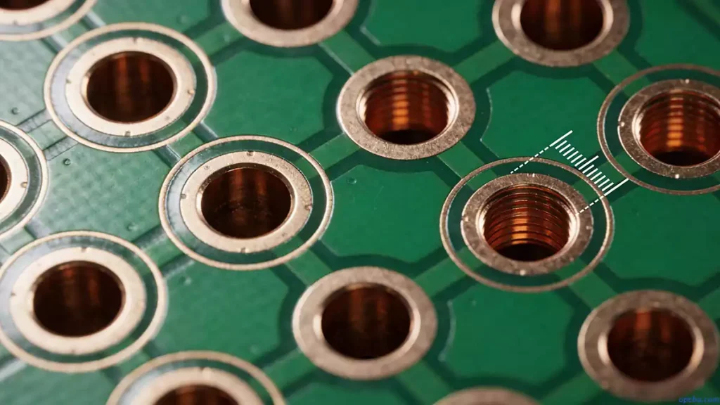
1.2 PCB Drilling Size Specifications for Robot PCBA
Drilling size defines the hole diameter on your robotic circuit board.When setting hole sizes per design charts, add a small margin to the required diameter.Solder will fill part of the hole space during assembly, reducing the final usable diameter. This margin compensates for manufacturing tolerances.
Ensure drill holes are at least 0.010 inches away from traces, copper planes, or pads.The minimum hole diameter must not be less than 0.008 inches to avoid manufacturing failures.
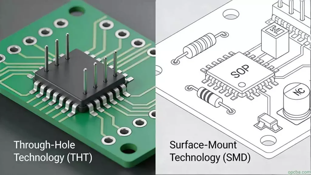
1.3 Robot PCBA Packaging & Layout Design
Always unpack and verify the package view during the design process.Generate a bottom view for manufacturer package validation. If using a top view, mirror the design to ensure component symmetry.
Maximize limited board space by using both sides of the assembly. For example: place surface-mount devices (SMDs) on the bottom, and through-hole components on the top.Use compact connectors where needed to save space for high-density robotic applications.
2. Key Challenges for Robotics Control Boards & Mitigation Strategies
Robotic control assemblies face unique performance and reliability challenges in robotic applications. These boards must deliver stable operation in dynamic, high-vibration, and even safety-critical environments. Risk mitigation is non-negotiable, especially for robot applications that impact human life or operational safety.
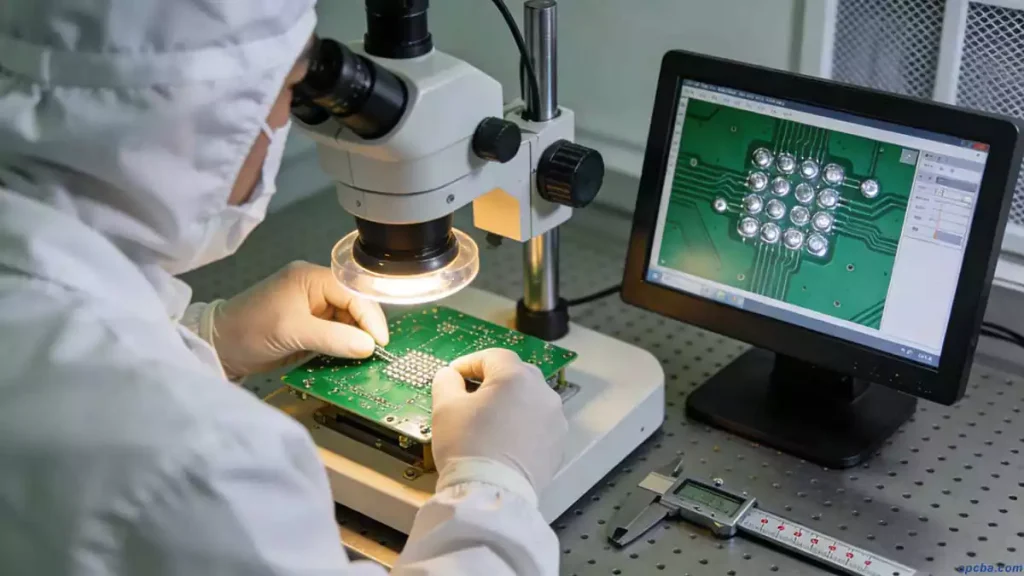
2.1 Robot PCBA Quality Assurance & Compliance
Robotic circuit assembly quality depends on strict manufacturing processes and standardized quality assurance.Partner with PCB suppliers with ISO 9001:2015 certification.
Ensure your supplier complies with industry-specific standards, including IPC-6012 and IPC-A-600.Adherence to these global standards guarantees consistent quality and reliability of your finished assembly.
2.2 Robot PCBA Design Risk Management
Mitigating design risks is a core challenge for robotic control board development.Mandate a design for manufacturability (DFM) review before production. This step validates the board’s design and avoids manufacturing failures.
Use design rule check (DRC) tools to verify the full design before engineering prototyping.DRC checks trace spacing, aspect ratio, open circuits, short circuits, and other critical design flaws.Addressing these issues early eliminates costly rework and design failures in mass production.
3. FAQ About Robot PCBA
Q: What is the main function of robot PCBA?
A: This robotic control assembly serves as the core control unit of a robot, governing motion control, sensor signal processing, power management, and communication between robotic components.
Q: What standards must robot PCBA comply with?
A: High-quality robotic control boards should meet global manufacturing standards, including ISO 9001:2015, IPC-6012 (rigid PCB qualification), and IPC-A-600 (PCB acceptability criteria).
Q: How to avoid thermal damage to robot PCBA?
A: Optimize wiring width for power and ground traces, use high-Tg PCB materials, and add thermal vias for heat-generating components to prevent thermal damage during long-term operation.
Robotic PCB assembly is the backbone of reliable robotic automation. By following strict design rules, complying with global manufacturing standards, and implementing proactive risk management, you can ensure your robot PCBA delivers stable, long-term performance in even the most demanding robotic applications.