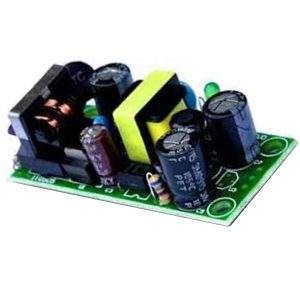
Description
Heavy copper PCB is a kind of special PCBs, its characteristic is its copper thickness is equal to or higher than 2oz. So, What is OZ? In the PCB industry, the unit of measurement used to express copper thickness is Ounce. 1oz in units of length represents the thickness of the copper foil of a PCB of approximately 36um, which is derived from the thickness of 1oz of 8.9g/cm^3 density pure copper laid out flat over an area of 1 sq. ft. (=144inches).
The PCB substrate is a copper-clad laminate, which in turn consists of substrate, copper foil, and adhesive. Generally speaking, the thickness of PCB copper foil is 0.5oz or 1oz. When the copper thickness of inner and outer layers of PCB is greater than or equal to 2oz, it is usually considered the heavy copper PCB.
1. What are the advantages of heavy copper PCBs over regular copper PCB?
The copper foil layer serves as a conductor of electricity on the board, allowing the copper layers on the board to work together to maximize their electrical performance. In the copper layer to realize the role of conductive at the same time, will generate heat, different thicknesses of copper corresponding to the difference in heat dissipation. Heavy copper PCB can carry more current, and reduce thermal strain, with better thermal performance.
(1) Heavy copper PCB can carry large currents.
Under a certain line width, increasing the copper thickness is equivalent to increasing the cross-sectional area of the circuit, which can carry more current.
(2) Heavy copper PCB reduce thermal strain
Copper foil has a smaller coefficient of conductivity, through the high-current case of temperature rise is smaller, so you can reduce the amount of heat, thereby reducing the thermal strain - refers to when the material is subjected to heat, due to the rise or fall in temperature, the geometric shape of the relevant aspects and dimensional changes that occur. Conductivity is the resistivity, metal "conductor" according to the conductivity coefficient of conductivity is divided into order: silver → copper → gold → aluminum → tungsten → nickel → iron.
(3) Heat dissipation of heavy copper PCB is good
Copper foil has a high thermal conductivity (thermal conductivity of 401W/mK), and can play an important role in improving thermal performance. Thermal conductivity refers to the stable heat transfer conditions, 1m thick material, the surface temperature difference between the two sides of 1°C, in 1H, through 1m2 area of heat transfer, unit W/m-K. This also greatly reduces the risk of burning boards and is an excellent option for high-current PCB design.
In addition, heavy copper PCB has thickened copper in the PTH and sidewalls, which improves the mechanical strength of the components and connections, and to a certain extent improves the synergy between components and PCBs, as well as reducing the size of the end product and other advantages.
2. What are the processes that require special attention when producing heavy copper PCB?
According to the above-mentioned, the copper thickness of PCB substrate is generally 0.5oz and 1oz. To achieve the copper thickness required by the customer (more than 2oz), it is necessary to use the electroplating process to electroplate the thickness of copper foil of the substrate to the required thickness, which is called copper plating.
After completing the plating process for the required copper thickness, the PCB needs to be etched to achieve the electrical performance designed by the customer. In the etching of thick copper lines, etching solution down the etching at the same time will be accompanied by a certain degree of side etching. The thicker the copper etching time will be, the more serious the side corrosion, and the line into a trapezoidal probability will be greater. To avoid the etching of the line becoming thin, before production, the production department will base on the thickness of the finished PCB copper line to compensate for certain. So in the design of heavy copper PCB, hardware engineers need to increase the line spacing to ensure that the line compensation process is in the production process, otherwise, the line spacing is too small, exposure development and line etching will lead to the line is too thin or open circuit.
In general, the special process of heavy copper PCB production:
(1) Electroplating: both the inner and outer layers need to be thickened by electroplating the base copper, increasing the thickness of the copper thickness of more than 2 OZ; for thick copper, the board is designed with a very high degree of integration, the thickness-to-diameter ratio of more than 10:1, the difficulty of immersed copper plating is high.
(2) Etching: inner and outer line etching is difficult.
(3) Resin-filling of the inner layer is required before press-fit.
(4) Soldermask needs to be printed many times.
3. Application areas of heavy copper PCB
Based on the advantages that heavy copper PCB can carry high currents and have good heat dissipation performance, heavy copper PCBs are favored by most product manufacturers of high-power devices, such as power supplies, solar panel devices, medical, automotive, aviation, and welding equipment manufacturers, etc. Heavy copper PCBs are widely used in a wide range of fields.
分享到: