Description
What’s Probe Card PCB?
Probe Card is the interface between the chip under test and the tester in the wafer test, which is mainly used for preliminary measurement of the electrical performance of the chip before chip packaging and screening out the defective chips before the subsequent packaging project. Probe Card consists of multi-layer PCB probes and functional components, with complex structures, according to different situations, there will be electronic components, reinforcement board (Stiffener), and other needs. The cantilevered probe card also contains rings, epoxy, etc. Storage conditions for probe card: Vacuum packed at the factory, unused probe card should be stored in a nitrogen cabinet with 25% +/-2% humidity.
In a word, the probe card is a test interface instrument mainly for bare-core testing.
Probe cards are categorized according to their structure: Blade cards, Cantilever cards, Vertical cards, Membrane cards, and MEMS cards.
MEMS: To improve throughput and develop a finer pitch (fine pitch), higher pin counts (high pin counts) of the probe card technology, micro-electromechanical process (Micro-Electrical-Mechanical Systems; MEMS) technology appeared, breaking through the Epoxy ring probe card (Epoxy) to manual one by one. The emergence of Micro-Electrical-Mechanical Systems (MEMS) technology breaks through the limitations of the Epoxy probe card (Epoxy probe card) by assembling the probes one by one manually and the Micro-spring probe card (Micro-spring probe card) by welding technology one by one, with a high degree of automation, breaks through the limitations that the production cost and the number of pin counts are proportional to each other and facilitates the production of the high number of probes. It is suitable for high pin counts (~30k pins/card), high currents, and high probe compression stroke testing needs. It maintains excellent stability and very low test scratches. In other words, even on very narrow-pitch wafers, there are only minimal scratches, which effectively increases durability and reduces the frequency of needle changes.
An integrated circuit (IC) is a semiconductor manufacturing process in which many transistors, resistors, capacitors, and other components are fabricated on a small silicon wafer and assembled into a complete electronic circuit using a multilayer wiring method.
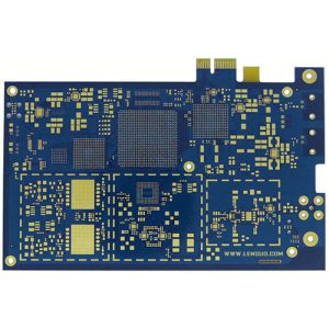
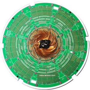
OPCBA.COM can produce a probe card PCB, from the above can be seen that the Probe card PCB is to carry the needle, ring, functional components of the carrier, and the realization of the tip of the needle and the signal transmission of the test machine, its shape, size and so on by the interface mode constraints, the material is subject to the constraints of the test environment, the corresponding shape is generally square and round. That refers to Probe card PCB.
Share an article about the development and application of probe card PCB.
The manufacturing process of the semiconductor industry can be divided into four major steps: IC design, wafer process, wafer test, and wafer packaging. One of the so-called wafer tests, that is each grain on the wafer electrical characteristics of the test, to detect and eliminate unqualified grains on the wafer.
1. Wafer test equipment “fingertip”-probe card
A wafer test equipment “fingertips” – probe card
Wafer testing is mainly through the linkage of the test machine and the probe station, in the test process, the test machine can not directly measure the wafer to be tested, but through the probe card (Probe Card) in the probe (Probe) and the wafer on the welding pad (Pad) or bump (Bump) contact and constitute electrical contact, and then through the probe measured test signals to the Automatic Test Equipment (ATE) for analysis and analysis of the wafer test equipment. The test signal measured by the probe is then sent to the automatic test equipment (ATE) for analysis and judgment so that the electrical characteristics of each die on the wafer can be obtained test results.
The probe card is an important part of the semiconductor wafer test process and is considered to be the “fingertip” of the test equipment. As each chip pin arrangement, size, pitch changes, frequency changes, test current, and test machine is different, different chips need to have a customized probe card, the current market does not have a type of probe card that can fully meet the test requirements. At the same time, for a mature product, when the production grows, the test demand will also increase, and the consumption of the probe card will also increase exponentially.
2. LTCC/HTCC technology in the application of the probe card
The probe card is the core component in this segment of wafer and chip testing, which provides the electrical connection between the wafer/silicon chip and the test instrument. The STF substrates are the core components in the entire probe card. The STF substrates function as the electronic connection pitch conversion and electrical signal transmission throughout the Probe Card while providing sufficient mechanical/mechanical strength to support the hundreds to thousands of Newtons of force applied during the test process.
The probe card (probe card body) is affected by the substrate material and is subject to deformation in multi-temperature (-55°C to 150°C) environments, especially at high and low temperatures. The probe is directly assembled on the probe card, and the deformation of the probe card causes the probe trace (the trace left when the probe makes contact with the wafer during wafer testing) to shift. The offset of the trace usually causes the probe on the probe card to make poor contact with the PAD (pad) of the wafer, resulting in unstable testing, and affecting test time and quality. If the trace offset is too large, the contact between the probe and the PAD of the wafer will damage the internal circuitry of the wafer, resulting in scrap and economic loss. At the same time, the probe card will also be scrapped because of the inability to carry out wafer testing.
Precision ceramic substrates have excellent electrical insulation, high thermal conductivity, high adhesion strength, and large current-carrying capacity. The temperature range of use is wide, which can reach -55℃~850℃, and the coefficient of thermal expansion is close to that of silicon chips. It is one of the effective solutions for deformation in multi-temperature test environments.
In addition, with the maturity and enhancement of technology, the chip function gradually increases, the design is gradually complex, and the number of chip input/output pins also continues to increase. To reduce production costs, the wafer size also continues to increase (such as 12-hour wafers), so the demand for large-area probe cards for detection is gradually increasing. For these large-area probe cards, due to the small pitch of the probe contact points, the structure usually utilizes a multilayer substrate (such as a multilayer ceramic substrate) with lines set between multiple probes and the circuit board as a spatial conversion device for the lines.
Probe card with ceramic substrate is generally a single film with metallization or multi-layer film ceramic multilayer substrate, multilayer ceramic substrate is a high-temperature or low-temperature co-fired ceramics through the multi-layer lamination, after co-firing production, usually called the multilayer ceramic space conversion substrate (multi-layer ceramic, MLC). Currently, suppliers are mainly Japanese and Korean companies such as Kyocera, NTK, SEMCNS, LTCC Materials, etc.