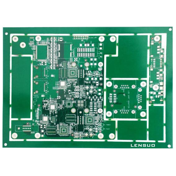
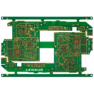
Description
Multilayer PCB consists of more than two conductive layers (copper layers) stacked on top of each other. the copper layers are bonded together by a resin layer (semi-cured sheet), and perforations are the source of electrical connections between the different layers of the multilayer PCB. The increased density of integrated circuit packages has led to a high concentration of interconnects, prompting multilayer PCBs to become the dominant trend in consumer electronics.
The biggest difference between multilayer PCB and single- and double-sided PCB is that multilayer PCB adds internal power and ground layers. multilayer PCB wiring is based primarily on the top and bottom layers, supplemented by intermediate wiring layers. The benefit can make corrections to the signal lines, but also better shielding interference. The focus of designing a multilayer PCB is on how to optimize the wiring of the internal electrical layers to make the circuit board wiring more reasonable.
1. Process Flow of Multilayer PCB
Customer Documentation - Documentation Review - Engineering Processing - Inner Layer Opening - Inner Layer Graphics Transfer - Etching - Desoldering - Brownout - Laminating - Drilling - Copper Immersion / Board Plating - Outer Layer Graphics Transfer - Graphics Electroplating Copper - Desoldering - Etching - Desoldering - Solder Resist - Solder Resist Imaging - Character Printing - Tin Blowing - Form Factor Processing - Testing - Final Inspection - Packaging
2. Four difficulties in the production and processing of multilayer PCB
(1) Difficulties in making inner-layer circuits
Multilayer PCB lines have various special requirements such as high speed, thick copper, high frequency, and high Tg value, which requires more and more requirements for inner layer wiring and graphic size control. For example, in ARM development boards, the inner layer has a very large number of impedance signal lines, to ensure the integrity of the impedance increases the difficulty of the inner layer line production.
The inner layer of signal lines, line width, and spacing are basically around 4mil or less; board layers of core board thin production are easy to wrinkle, these factors will increase the production cost of the inner layer.
(2) Difficulty of alignment between inner layers
With more and more layers of multilayer PCB, the alignment of the inner layer is also more and more demanding. Films by the workshop environment temperature and humidity will have the effect of rise and fall, the core board will have the same rise and fall, which makes the precision of the alignment between the inner layer more difficult to control.
(3) Difficulties in pressing process
Multiple core boards and PP (semi-cured sheet) superposition, in the press-fit is prone to delamination, slippery boards steam bag residue, and other problems. The number of layers is large, and the control of rise and shrinkage and the compensation of size coefficient can not maintain consistency; the thin insulation layer between the layers is prone to lead to the failure of the inter-layer reliability test.
(4) Difficulties in drilling production
Multilayer PCB using high Tg or other special plates, different materials drilling roughness is not the same, increasing the difficulty of removing glue residue in the hole. High-density multilayer PCB hole density, low production efficiency, easy to break the knife, different networks over the hole between the hole, and the hole edge being too close will lead to CAF effect problems.
3. Why are multilayer PCBs often an even number of layers?
(1) Odd-layer PCBs are easier to bend. When the PCB is cooled after the multilayer bonding process, the PCB bends due to the inconsistency of the lamination tension between the core structure and the foil-laying structure. The key to eliminating bending is to use a balanced laminate stack, even number of layers PCB is symmetrical, the degree of warpage can be controlled below 0.7%; but odd number of layers PCB, especially when the size is large, the degree of warpage will be more than 0.7%.
(2) Even layer stacking design helps to improve the PCB anti-jamming ability. PCB signal layer and ground layer (or power supply layer) generally appear in pairs, so that the device can be shielded from signal interference. Such as the common 6-layer board layer order: SIG-GND-SIG-PWR-GND-SIG. A core board is on both sides of the copper, that is, both sides can be done line, made into an odd number of layers means that there is a layer of empty, and if you do not use is a waste. Therefore, for any EMI engineers, this layer will be designed as a power layer or ground layer to play a shielding role.
(3) Special processes are difficult to ensure the yield, so the yield of the odd-numbered layer PCB is often lower than the even number of layers.
4. Advantages of multilayer PCB:
Multilayer PCB has durability, functionality, and lightweight.
(1) High assembly density, small size, lightweight, to meet the needs of electronic equipment lightweight miniaturization
(2) Increase the number of wiring layers, increasing the design flexibility;
(3) Due to the high assembly density, the connection between the components (including components) is reduced, simple installation and high reliability;
(4) Multilayer PCBs allow products to gain more functionality, and their high assembly density extends the service life of the board, and the electrical characteristics are faster than those of single-layer boards.
(5) As the graphics have repeatability and consistency, it reduces wiring and assembly errors and saves time for equipment maintenance, debugging, and inspection;
(6) The ability to form circuits with a certain impedance allows the formation of high-speed transmission circuits;
(7) Can be set up the circuit, magnetic circuit shielding layer, can also be set up metal core heat dissipation layer to meet the shielding, heat dissipation, and other special functional needs.
5. Multilayer PCB applications
With the continuous development of electronic technology and computer, medical, aviation, and other industries electronic equipment requirements continue to improve, the circuit board is shrinking in size, reducing the quality, and increasing the density of the direction of development. Single- and double-sided printed circuit boards due to the limitations of the available space, it is not possible to achieve a further increase in assembly density, so it is necessary to consider the use of more layers, and assembly density of higher multilayer circuit boards. Multilayer circuit board with its flexible design, stable and reliable electrical performance, and superior economic performance, has been widely used in the manufacture of electronic products.
(1) Computer
(2) Heart monitor
(3) Fire alarm
(4) GPS and satellite systems
(5) Industrial control
分享到: