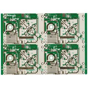
Description
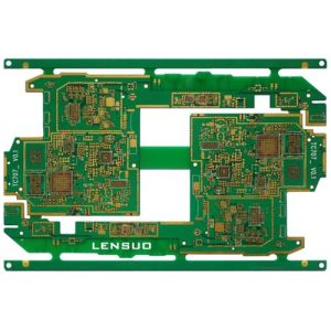
HDI PCB, High-Density Interconnector PCB refers to the use of HDI technology, containing micro vias, blind vias, and buried vias with a high density of line distribution. HDI PCB contains inner and outer layers of wires and then uses vias and metalized holes to achieve the function of bonding between each inner layer to achieve the electrical performance of the entire PCB. Compared to standard PCBs, HDI PCBs have thinner wires and spacing, smaller through holes and capture pads, and higher connection pad density. HDI PCBs are used to reduce size and weight, as well as to enhance the electrical performance of devices.
With the development of high-density and high-precision electronic products, the requirements of the boards are getting higher and higher. To increase their high-density performance, the most effective way is to reduce the number of through holes and set up blind and buried holes accurately.
1. Types of holes involved in HDI PCBs
(1) micro-hole: aperture diameter of 0.25mm or less can be referred to as a micro-hole, the commonly used method of turning holes in mechanical drilling, CO2 laser drilling, UV laser drilling three kinds of holes (general aperture diameter of 0.1mm and above the through-hole more than the use of mechanical drilling, 0.1mm and the following blind holes more than the use of laser drilling).
(2) blind holes: blind holes are connected to the surface layer and the inner layer and not through the whole plate of the guide hole. In the top or bottom layer of which a layer can be seen, the other layer can not be seen. In machining, for two or more parts of the connection.
(3) buried holes: PCB internal links between any circuit layers but not through to the outer layer, do not extend to the surface of the circuit board through holes.
2. HDI PCB features
(1) Smaller size and lighter weight. It is made by pressing a conventional double-sided board as a core board through a base layer. Electrical interconnections between the layers are realized through conductive through-hole, buried holes, and blind hole connections, so the number of layers and the aspect ratio are often reduced, with “light, thin, short, small” and other advantages.
(2) HDI wiring density. Its high density is mainly embodied in the hole, line, pad density, and interlayer thickness, HDI board contains blind holes and other micro-conductor hole designs, which is mainly manifested in the aperture less than 150um micro-hole into the hole technology, as well as cost, production efficiency and hole precision control and other aspects of the high demand for chemical. Ordinary multilayer circuit boards only through holes and there are no tiny buried blind holes.
Line width and line spacing of the refinement of the main performance in the wire defects and wire surface roughness requirements are increasingly stringent, with the general line width and line spacing of no more than 76.2 um. Pad density is high, the density of welded joints per square centimeter is greater than 50. Thin dielectric thickness is mainly manifested in the interlayer dielectric thickness to 80um and below, the thickness uniformity requirements are becoming more and more stringent, especially for the characteristic impedance control of high-density boards and packaging substrates.
(3) Better electrical performance
Terminal product design is more miniaturized to meet the higher standards of electronic performance and efficiency. HDI’s increased interconnect density allows enhanced signal strength and improved reliability. In addition, the HDI board for radio frequency interference, electromagnetic wave interference, electrostatic discharge, heat conduction, etc. has better improvement. HDI also adopts full digital signal process control (DSP) technology and several patented technologies, with a full range of adaptive load capacity and strong short-term overload capacity.
(4) High requirements for buried hole plugging
3. HDI PCB advantages
(1) can reduce the cost of PCB: when the density of PCB increases by more than eight layers of the board, to HDI to manufacture, its cost will be lower than the traditional complex compression process.
(2) increase line density: traditional circuit boards and parts of the interconnections
(3) Favor the use of advanced assembly technology
(4) Better electrical performance and signal integrity
(5) Better reliability
(6) Improved thermal properties
(7) can improve radio frequency interference / electromagnetic wave interference / electrostatic discharge (RFI / EMI / ESD)
(8) Increase design efficiency
4. Relevant standards
(1) IPC-2226 Sectional Design Standard for High-Density Interconnect (HDI) Printed Boards
(2) IPC-2221 Generic Standard on Printed Board Designs
5. Application of HDI PCB
Electronic designs are constantly improving the performance of the entire machine while trying to reduce its size. In small portable products from cell phones to smart weapons, “small” is the constant pursuit. High-density integration (HDI) technology can make the end product design more miniaturized while meeting the higher standards of electronic performance and efficiency. HDI is currently widely used in cell phones, digital (camera) cameras, MP3, MP4, notebook computers, automotive electronics, and other digital products, etc., which are most widely used in cell phones.
HDI boards are generally used in the accumulation of layers (Build-up) manufacturing, the more the number of layers, the more the board is used, and the more the board is used. HDI boards are generally manufactured using the build-up method, and the more the number of layers, the higher the technical grade of the board. Ordinary HDI board is a 1-time layer, high-level HDI using 2 or more times the layer technology, while the use of stacked holes, plating to fill holes, laser direct punching, and other advanced PCB technology. High-order HDI boards are mainly used in 3G cellular phones, advanced digital cameras, IC carrier boards, etc.