PCB Layout refers to the rational arrangement of electronic components and routing of connections on a circuit board. Done properly, it directly lifts circuit performance, lowers production costs, and creates a more reliable end product.
Poor layout, by contrast, often leads to signal interference, instability, or even functional failure. For a high-performance, cost-effective bare PCB board, every step of the layout process matters.
Starting Points of PCB Layout Design
In real engineering practice, PCB layout always begins with board size. The final dimensions must match the product enclosure and assembly requirements, as an oversized or undersized board will hurt both performance and manufacturability.
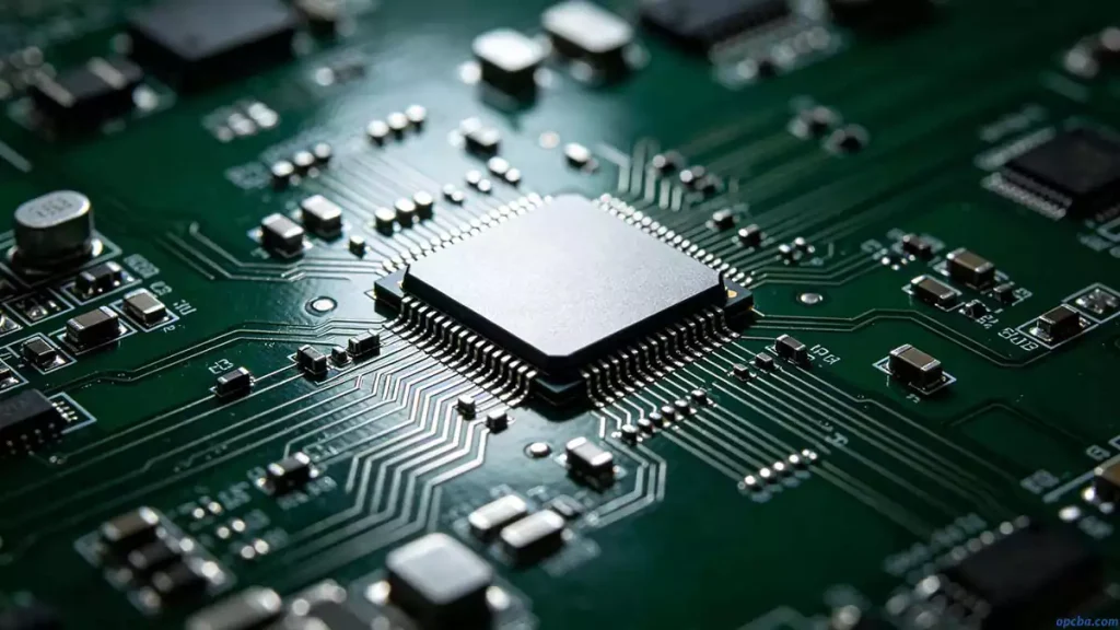
Once the board outline is fixed, designers next position special components. These include high-frequency parts, core circuit devices, and high-voltage components.
Only after placing these critical parts do we arrange the remaining standard components based on circuit function and signal flow.
Why Special Component Placement Matters
Special components often dictate whether a design works as intended. Placing them incorrectly can create signal integrity issues, electromagnetic interference, or compatibility problems that ruin the entire design.
Getting these positions right is one of the most decisive steps in PCB Layout. It needs to align with both electrical function and real-world production and assembly constraints.
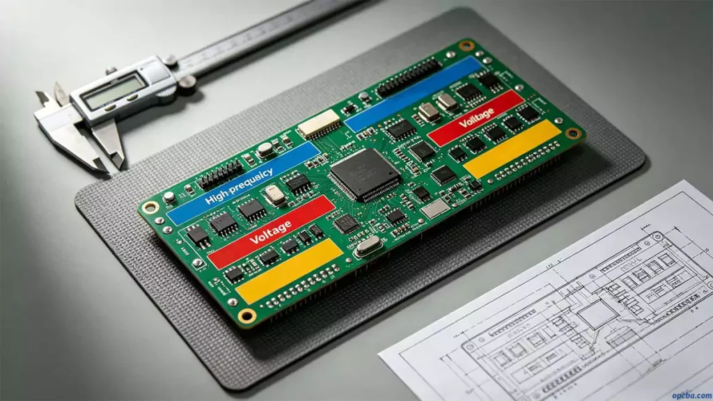
Key Layout Guidelines to Follow
- Keep connections between high-frequency components as short as possible. This reduces stray parameters and lowers the risk of electromagnetic interference during operation.
- Separate noise-sensitive components from input and output areas. Placing them too close often leads to signal distortion and unstable performance.
- Increase clearance between parts with high potential differences to avoid arcing or short circuits. High-voltage components should be positioned away from easily accessible areas for safety.
- Components heavier than 15 grams require mounting brackets and reinforced soldering. Heat-generating and heavy parts also perform better when placed near the main chassis base for improved stability and cooling.
- Keep temperature-sensitive components away from heat-dissipating devices to prevent thermal drift and premature failure.
- Adjustable components should be placed with the final product structure in mind, making calibration or adjustment practical.
- Place frequently used controls and switches within easy reach, where users or technicians can access them comfortably.
A strong layout doesn’t just follow rules — it balances performance, density, and mechanical stability across the entire bare PCB board.
The goal is to create a design that is electrically clean, easy to assemble, and consistent in quality during mass production.
To clarify the key differences between bare PCBs and fully assembled PCBA, explore our detailed comparison guide: PCB vs PCBA: Key Differences and Definitions
If you need professional manufacturing support for your finished layout designs, opcba can produce high-quality bare PCB boards tailored to your specifications.


