SMT Surface Mount Technology is a foundational electronics manufacturing process. It creates smaller, lighter electronic products. It also cuts production costs. This guide explains its core basics, history and key terms. It helps you understand this critical PCB assembly method.
What is SMT Surface Mount Technology?
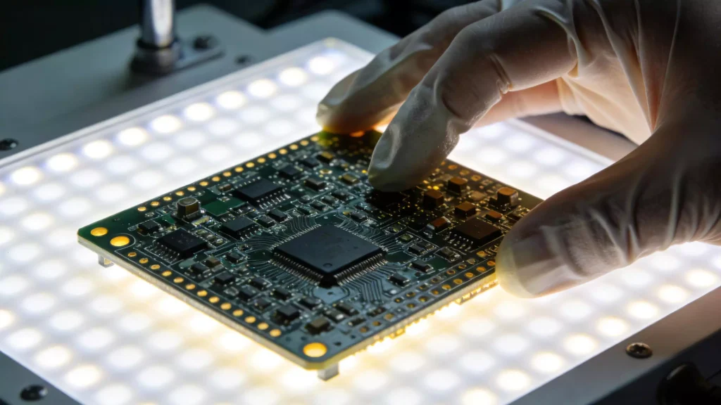
SMT Surface Mount Technology is a key electronic packaging technique. It mounts components directly onto PCB surfaces. This is different from old through-hole technology (THT). THT uses pre-drilled holes for component leads.
It powers modern microelectronics. It is the standard for phones, industrial controls and car electronics. It supports high-density component placement.

The History of SMT Surface Mount Technology
SMT Surface Mount Technology started in the 1950s and 60s. It grew from Flat Packs and hybrid microelectronics. Early versions set the stage. Today’s technology is always evolving. It focuses on smaller size and higher density.
Fine pitch, UFP and BGA components are now common. Advanced methods like COB, TAB and flip chip are widely used. For top performance, Multi Chip Modules (MCM) are an option. They need precise SMT Surface Mount Technology skills. They cost more than standard SMT.
Key SMT Terminology & Definitions (A-C)
Understanding SMT Surface Mount Technology terms ensures quality PCB assembly. Below are essential terms, sorted alphabetically for easy lookup.
A-Class Terms
A1: Resin & Cleaning Basics
- A-stage: Resin in its low molecular weight state. It melts and dissolves easily. It is critical for SMT-compatible PCB materials.
- Aqueous cleaning: A water-based method for SMT assemblies. It may use neutralizers or just deionized water. It is eco-friendly.
- Azeotrope: A mix of polar and non-polar solvents. It acts as one solvent to clean contaminants. It has a fixed, low boiling point.
A2: PCB Structure & Materials
- Anisotropy: A material (Z-axis glue) with few conductive particles. It conducts electricity only vertically (Z-axis). It does not conduct horizontally (X/Y axes).
- Annular ring: Conductive material around a PCB drilled hole. It connects the hole to circuit traces. It ensures reliable electrical contact.
- Aspect ratio: The ratio of PCB thickness to hole diameter. Holes with a ratio over 3 often crack in SMT processing.
B-Class Terms
B1: Components & Connections
- B-stage: Resin-impregnated sheets (like glass fiber). They are cured to an intermediate state. They are used for rigid-flex PCBs in SMT.
- Ball Grid Array (BGA): An IC package with solder ball I/O points. The balls form a grid pattern. It is essential for high-density SMT Surface Mount Technology.
- Butt joint: A sheared lead from an SMD component. The lead end touches the PCB pad directly. It is a standard SMT connection.
B2: Defects & PCB Features
- Blind via: A hole from an inner PCB layer to the surface. It does not go through the whole board. It saves space for high-density mounting.
- Porosity: Gaps in solder joints from fast degassing. It happens during soldering. It weakens joint reliability.
- Bridge: Solder that connects two unrelated conductors. It causes electrical short circuits. It is a major SMT defect.
- Buried via: A hole connecting inner PCB layers. It does not reach the surface. It is used for ultra-high-density assembly.
C-Class Terms
C1: Resin, Heating & Environment
- C-stage resin: Resin cured to its final rigid state. It gives PCBs structural stability after SMT processing.
- Capillary action: The mix of adhesion, cohesion and surface tension. It pulls molten solder into tight spaces. It is vital for SMT soldering.
- CFC (Chlorofluorocarbon): Ozone-damaging chemicals. They were once used in SMT cleaning. They are now banned globally.
C2: Quality & Performance
- Castellation: Metallized semicircles on LCCC edges. They connect component surfaces to PCB pads. They are used in lead-free chip carriers.
- Characteristic impedance: The voltage-to-current ratio of a PCB trace. It depends on trace width and dielectric material. It matters for high-speed SMT.
- Chip component: Small, leadless passive parts (like resistors). They are the most common components in SMT Surface Mount Technology.
C3: Advanced Processes
- Chip on Board (COB): Mounts unpackaged silicon chips directly on PCBs. Connections use wire bonding or flip chip. It is an advanced SMT derivative.
- CLCC: Ceramic leadless chip carriers. They are used for high-reliability SMT assembly. They are common in industrial electronics.
- Condensation reflow soldering: Uses hot, oxygen-free steam to heat SMT assemblies. Steam condenses on cool parts. It transfers heat evenly.
C4: Defects & Metrics
- Cold solder joint: A defective joint from low heat or impurities. It looks gray and porous. It has poor electrical conductivity.
- Column Grid Array (CGA): An IC package with solder column I/O points. It offers better stability than BGA. It is used in harsh environments.
- Contact angle: The angle between solder and a pad. Angles under 90° are good for SMT. Angles over 90° mean poor wetting.
- CTE (Coefficient of Thermal Expansion): The rate a material expands with heat. Matching PCB and component CTE prevents thermal damage.