SMT Reflow & Wave Soldering for Lead-Free PCBA are the foundational processes in modern electronic manufacturing. They create reliable, durable solder joints for lead-free printed circuit board assemblies (PCBAs). This guide breaks down their core mechanics and practical optimization tips for production efficiency.
What is SMT Surface Mount Technology?
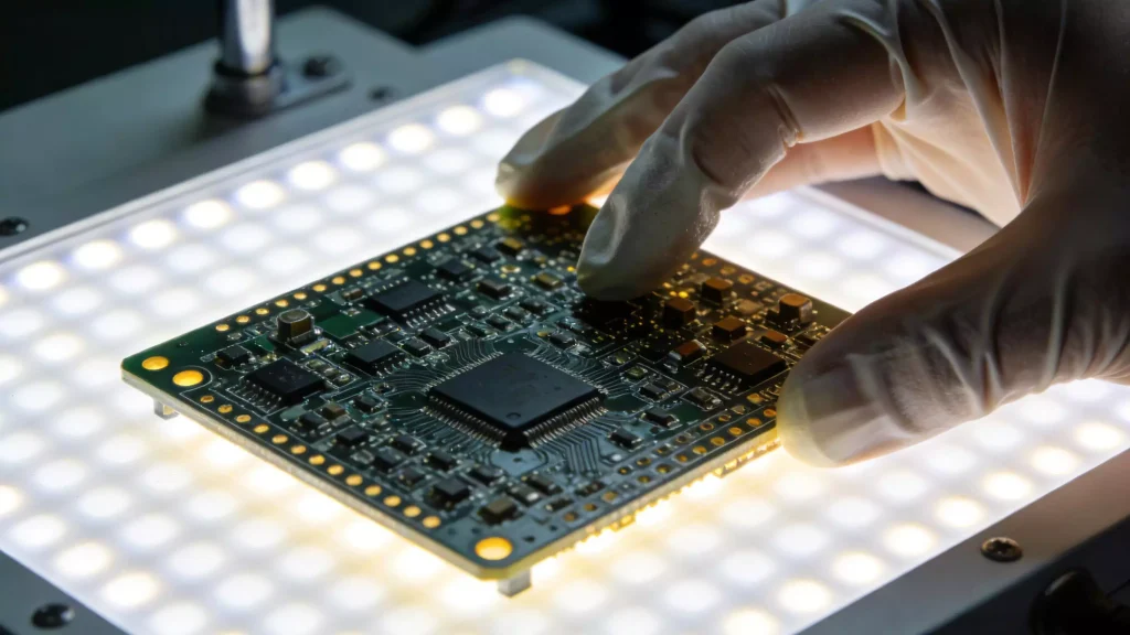
SMT Surface Mount Technology is a key electronic packaging technique that mounts components directly onto PCB surfaces—distinct from traditional through-hole technology (THT), which uses pre-drilled holes for component leads. It is the backbone of modern microelectronics, serving as the standard for phones, industrial controls, car electronics, and other devices that require high-density component placement.
Core Principles of Reflow Soldering for Lead-Free PCBA
Reflow soldering is the backbone of SMT lead-free soldering processes. It uses controlled heat to melt pre-applied solder paste, forming strong bonds between components and the PCB surface. It is the most widely used method for high-volume SMT assembly, adapting to lead-free manufacturing requirements.
Batch vs. In-Line Furnaces
Two main furnace types cater to lead-free PCBA soldering workflows:
- Chamber (Batch) Furnaces: Load full PCB batches at once. They offer precise control over temperature and atmosphere, including vacuum. They are ideal for small-batch production and complex PCBs.
- In-Line (Conveyor) Furnaces: Integrate into continuous production lines. They use 5–7 heating zones for uniform temperature distribution. They are the top choice for high-volume manufacturing.
Key Furnace Selection Factors
Choosing the right furnace depends on two core factors for lead-free production:
- Throughput Needs: In-line furnaces handle thousands of PCBs daily. Chamber furnaces excel at low-volume, high-precision jobs.
- Thermal Control: Complex PCBs need extra heating zones to prevent thermal shock. This protects sensitive components and ensures consistent results.
Lead-Free Challenges in SMT Reflow Soldering
Lead-free alloys have transformed modern SMT soldering operations. Their higher melting point (217°C vs. 183°C for tin-lead) requires adjusted temperature profiles to meet process standards.
Temperature Profile Types
Lead-free reflow uses two main profile types:
- Soak Profile: Includes a hold phase to activate flux. It heats components evenly to reduce thermal stress.
- Ramp-Soak-Spike Profile: Uses faster heating to minimize high-temperature exposure. This protects delicate parts.
Balancing Heat & Component Safety
Optimizing lead-free soldering requires careful balance. The temperature must melt solder under large components, but also avoid damaging small, heat-sensitive parts. Some complex PCBs need separate soldering steps for large components.
Wave Soldering for Hybrid Lead-Free PCBA
Wave soldering complements reflow in SMT Reflow & Wave Soldering for Lead-Free PCBA workflows. It is designed for hybrid PCBs with both SMT and through-hole components, providing reliable connections for through-hole parts that reflow cannot process.
Core Process Requirements
- SMT components on the wave side are fixed with adhesive. This prevents movement during soldering.
- Components must withstand peak temperature shocks from the molten solder wave.
- The PCB top surface stays below the solder solidus temperature. This avoids unwanted solder joints.
Equipment Options
- In-Line Wave Soldering: Integrates into production lines for high-volume runs. It supports continuous assembly workflows.
- Selective Wave Soldering: Targets specific PCB areas like connectors or transformers. It reduces thermal exposure and improves efficiency.
Warping Prevention
Wave soldering needs specialized PCB support. This prevents warping and ensures full contact with the solder wave. It is a key design difference from reflow equipment.
Lead-Free Impact on Wave Soldering
Lead-free technology has improved SMT lead-free soldering performance:
- Bath Temperature: Lead-free alloys use the same 250–270°C bath temperature as tin-lead solder. This minimizes equipment overhauls.
- Alloy Additives: Nickel and germanium are added to lead-free alloys. They create bright, aesthetically pleasing solder fillets.
- Corrosion Resistance: New equipment uses corrosion-resistant steel and ceramic coatings. These withstand the aggressive nature of lead-free alloys.
Practical Optimization Tips
SMT Reflow & Wave Soldering for Lead-Free PCBA relies on three key optimizations: matching furnace type to production scale, fine-tuning temperature profiles for alloy properties, and using anti-warping support for wave soldering. These steps ensure consistent yield and reliable solder joints, building on the foundational SMT technology knowledge outlined earlier.


