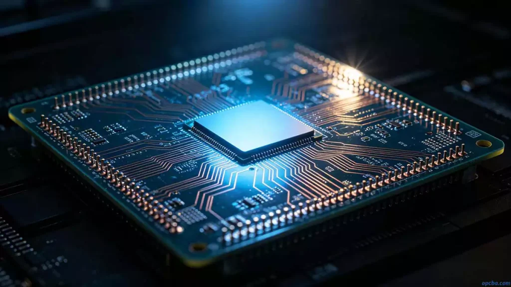
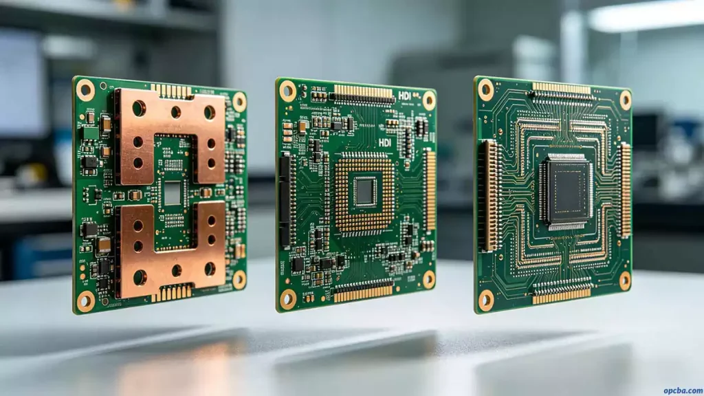
IC carrier board — also called a packaging substrate — is essentially a high-end PCB that acts as the signal bridge between a bare die and the main PCB. Unlike standard PCBs, these boards are built to connect directly to chips, so they demand far tighter precision.
Their evolution traces back to HDI technology: from ordinary PCBs to HDI, then to SLP, and finally to today’s IC carrier boards. Each step pushed processing accuracy higher, to meet the shrinking form factors and growing complexity of modern semiconductors.
Market Trends: What’s Driving Growth (and Where It’s Headed)
As core components of IC packaging, packaging substrate demand rises and falls with the semiconductor industry. 2021 marked a peak, as the global semiconductor boom pushed market growth to its highest level in a decade.
Downstream applications paint a clear picture of where demand comes from. PCs, servers, consumer electronics, and communications together make up 95% of the market. In 2021, PCs (high-performance CPUs/GPUs) led at $4.2 billion (29%), followed by phones (SoC/RF, $3.6 billion, 25%) and servers/storage ($2.4 billion, 17%). Combined, the top four applications accounted for 86% of share, with communications (wired + wireless) making up another 9%.
Moving forward, the PC boom driven by pandemic remote work is expected to cool, while consumer electronics will stabilize. The real growth driver will be server/storage chips, with wireless communications and automotive applications also outpacing average growth rates.
The Triple Barriers Keeping New Players Out
IC carrier board triple barriers — capital, technology, and customer — make this industry notoriously hard to break into.
First, the capital barrier is steep. Manufacturing is capital-intensive, relying on expensive imported equipment and requiring customers to audit production capacity before approving suppliers. New entrants face massive upfront costs with no quick path to ROI.
Technical barriers are just as tough. Unlike standard PCBs, these boards are smaller, with tighter line spacing, finer vias, and strict signal interference rules. Building them requires advanced layer alignment, plating, and drilling tech — plus years of process refinement. Consumer electronics demand thin, compact designs, while server products need extreme high-density interconnection, both requiring expertise across materials, chemistry, and mechanics.
Then there’s the customer barrier, which often flies under the radar. Most downstream clients are large semiconductor firms with strict qualification cycles. A single Samsung storage carrier board certification can take up to 24 months, with multiple trial phases before full orders kick in. Once qualified, clients rarely switch suppliers, leaving new entrants locked out.
Beyond Semiconductors: Where IC Carrier Boards Are Used
These high-precision substrates aren’t just for chips. Their small form factor, high density, and reliability make them ideal for aerospace, defense, and automotive electronics, where failure isn’t an option.
At OPCBA, we design and manufacture custom IC carrier board solutions for high-reliability applications. If you’re working on a project that needs these specialized substrates, reach out to discuss your requirements.


