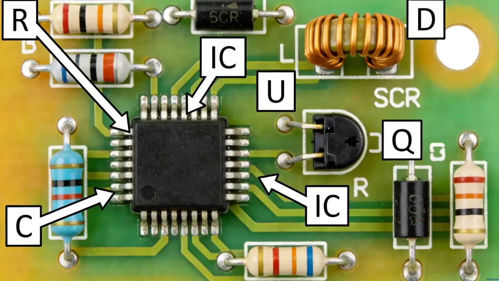
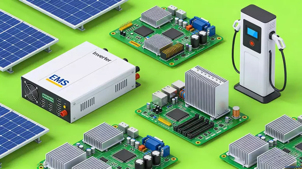
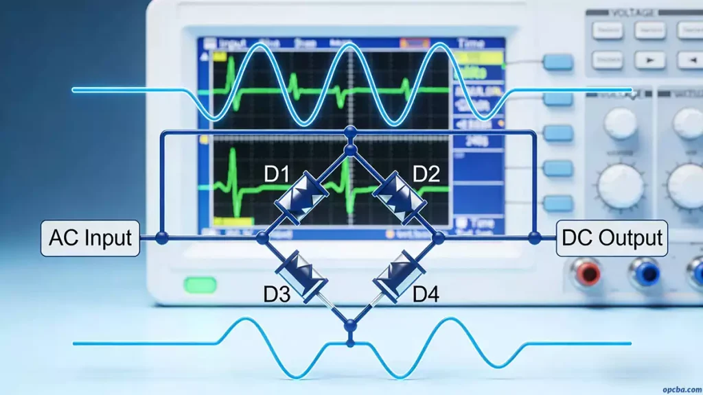
The keyboard acts as the primary input device for daily computing, used for typing, shortcuts, gaming, menu navigation and more. At the center of its internal structure lies the keyboard PCB, which serves as the control core of the entire unit.
Housed inside the keyboard assembly, it handles key scanning, signal encoding and interface transmission. It turns each keystroke, whether a letter, number or command, into a digital signal the computer can interpret, acting as a key bridge between user and device.
Common Types of Keyboards & PCB Designs
Keyboards are generally split into three categories by application: desktop, notebook and industrial keyboards. Desktop models are further divided by internal switch structure: mechanical and capacitive designs.
Mechanical keyboards rely on physical switch contacts, which tend to wear out, collect dust and degrade over time. For this reason, they have mostly been phased out in mainstream products.
Capacitive keyboards use non-contact sensing, which greatly improves reliability and service life. Today, most standard input keyboards use this capacitive-based keyboard PCB structure.
Mechanical vs Capacitive: What Changes on the PCB
Mechanical and capacitive keyboards look similar from the outside, but the board underneath them is a different design problem.
Mechanical switches are contact devices. Each switch shorts two pads together, so the contact plating has to survive repeated actuation, and the firmware has to debounce a signal that never closes cleanly. Metal contacts also make the switch pads a natural ESD entry point, which is why ground stitching and a properly routed ground plane matter on these boards.
Capacitive designs never make electrical contact. Each key sits above a sensing pad, and the controller reads a change in capacitance as the plunger approaches. That removes the wear problem, but it moves the requirement to the sensing electrode itself: pad geometry, trace routing and the dielectric layer above it all set the sensitivity, and inconsistent solder mask thickness across the board shows up as inconsistent key response.
How Matrix Keyboard PCB Circuits Work
A matrix keyboard PCB is the standard layout used in microcontroller-based input devices, arranging keys in a grid formation rather than a direct-wired setup. This design is more complex than direct wiring, but far more efficient for boards with many keys.
In this structure, column lines connect to positive power through pull-up resistors. Row lines link to microcontroller I/O ports as outputs, while column ports act as inputs. Each intersection only connects when a key is pressed, no direct contact otherwise.
This arrangement drastically cuts down on I/O port usage. A simple 4×4 grid creates 16 keys with just 8 ports, far more than direct wiring. The more keys required, the bigger the advantage becomes.
Matrix designs show up everywhere: calculators, remote controls, security keypads, ATMs and industrial input devices. For any product needing a high number of keys in a small space, this matrix layout is the most practical solution.
Ghosting, Blocking and NKRO: Why Diodes Matter
A matrix without diodes has a limit that only shows up when several keys are pressed at once.
Take a 2×2 section of a matrix: press three of the four keys and the controller can see a path that makes the fourth look pressed too. This is ghosting. Firmware cannot tell a real key from a phantom one, so most controllers respond by blocking the extra keys. Some key combinations simply will not register as a result, and the problem gets worse as the matrix grows.
The fix is a diode in series with every switch. Current can only travel one way through it, so the phantom path breaks. With that in place the controller can report any combination of keys at once, which is what NKRO (n-key rollover) means. Under the standard USB HID boot protocol a keyboard is limited to six keys plus modifiers, or 6KRO; reporting more requires a custom HID report descriptor, which is why some NKRO keyboards need a driver or a mode switch.
The part itself is not exotic. A 1N4148 or an SMD equivalent such as 1N4148W handles the current and switching speed of a keyboard matrix comfortably. What matters at layout is that each diode sits close to its switch and the direction stays consistent across the whole matrix.
Scan Rate, Debounce and Response Time
Matrix scanning is fast by design. The controller drives one row at a time and reads the columns, so a 5-row matrix needs five read cycles for a full scan rather than one per key. Full scans in the low kilohertz range are routine, and they leave plenty of headroom before the host polls the device.
What actually limits response is debounce. A mechanical contact bounces for a short period, typically 1 to 5 ms, before it settles, and firmware ignores transitions during that window. Set the window too short and a single press registers twice; set it too long and fast repeated taps get dropped. Capacitive designs have the opposite problem: there is no contact bounce to filter, but the sensing threshold needs its own settling time and drift compensation.
Neither figure is something a PCB designer sets directly, but both depend on the board. Pad finish and cleanliness affect how cleanly a mechanical contact closes, and electrode geometry sets how much margin the capacitive sensing threshold has.
Custom Keyboard PCB Support
If you’re building a custom mechanical or capacitive input device and need to produce your own matrix keyboard PCB, we can help. Simply send us your Gerber files. Our capability and process overview covers layer counts, surface finishes and assembly in one place.