Drawing on over 12 years of collaboration with hundreds of hardware engineering teams, we’ve watched more than one product launch derailed by teams cutting corners on PCB prototypes. The most memorable case was a 2022 smart home security camera project: the client’s team skipped prototype validation to hit a launch window, only to find 12,000 mass-produced boards had a 5V trace routing flaw that caused random reboots. The rework cost $45,000 and pushed the launch back 10 weeks.
These test boards are engineered to validate circuit functionality, thermal performance, and design manufacturability before locking in a mass production run. Even small oversights in differential pair length matching or via stitching can turn into systemic failures at scale, and prototype runs are the most consistent way to catch these flaws before they impact your bottom line.
Why Prototyping Directly Impacts Your Product’s Success
Industry benchmarks indicate that fixing a design flaw in the prototype phase costs an order of magnitude less than addressing it after mass production starts, as widely cited in design-for-manufacturability analyses. It also cuts down on costly launch delays, which can make or break a product in competitive consumer and industrial electronics markets.
Iterative PCB prototyping also drives meaningful design improvements. On a 2023 industrial IoT gateway project built around the STM32H743 main chip, we supported the client through 3 prototype rounds. Each iteration let us collaborate with their team to refine the power delivery network, reduce thermal rise on the PMIC by 18°C, and shrink the overall form factor by 12% without sacrificing performance.
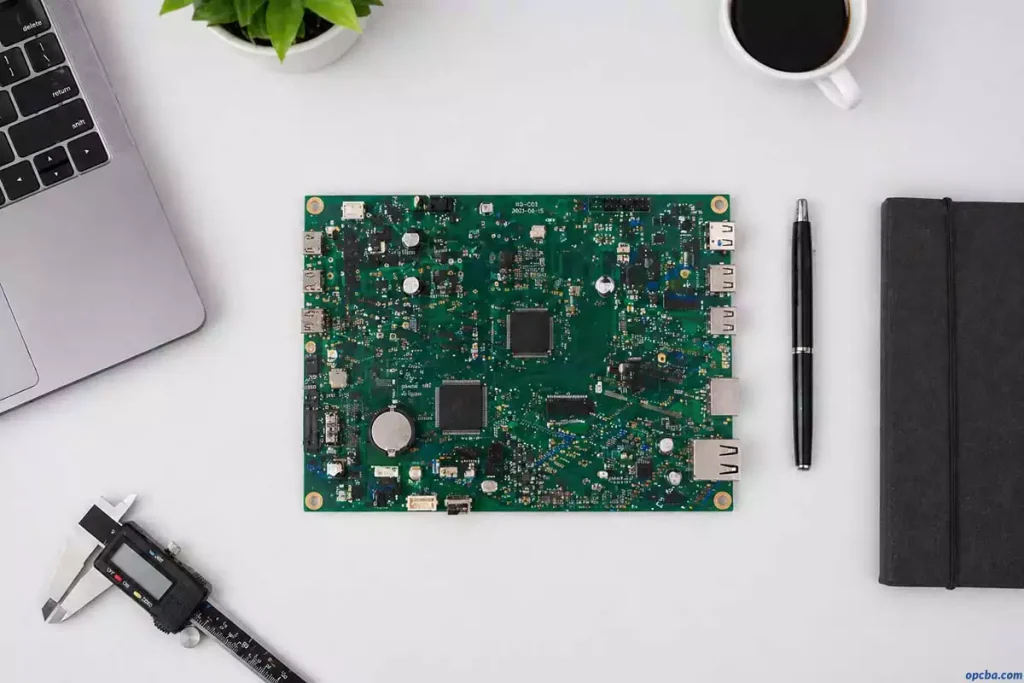
The Field-Tested PCB Prototyping Process We Use for Every Client Project
Every design has unique requirements, but we follow a standardized, IPC-aligned workflow for every PCB prototyping process to ensure consistent, reliable results for our clients.
Locking in the Design & Pre-Fabrication DFM Check
We start with the client’s complete schematic capture and PCB layout, built in tools like Altium Designer for high-speed designs or KiCad for lower-complexity projects. Before sending files to our fabrication line, we run a complimentary full Design for Manufacturability (DFM) check to flag trace spacing violations, undersized drill holes, solder mask clearance issues, and other flaws that will impact fabrication or assembly.
We build this step into every project timeline, as even a 0.05mm DFM error can make a prototype impossible to assemble, or lead to intermittent failures once components are mounted.
Fabricating the Prototype
Once the design is locked and passes DFM, we fabricate the prototype to match the same material stackup, fabrication process, and component specs as your planned mass production run. This ensures test results from the prototype will directly translate to your final production boards, rather than being skewed by different materials or processes.
For specialized designs, we adjust the workflow to match requirements: high-frequency RF boards get tighter impedance tolerance controls, while high-power industrial designs use thicker copper foil for better current handling. For instance, our facility maintains a controlled impedance tolerance of ±5% across all prototype runs. We keep high-frequency materials including Rogers 4350B and Panasonic Megtron 6 in stock, and support prototype builds up to 20 layers with a minimum line width/space of 3/3mil. To learn more about the core fabrication process that defines trace precision and board performance, read our full guide: Etching Process and Precautions
Structured Testing & Iterative Refinement
Once the bare boards come off our fabrication line and are assembled, we and the client’s engineering team run testing in a strict, standardized sequence to catch every potential flaw:
- Electrical Baseline Testing: We start with flying probe testing to verify continuity, isolation resistance, and controlled impedance matching for high-speed traces. This catches fabrication and assembly flaws like solder bridges, lifted pads, and via failures before the board is powered on.
- Functional Validation: Next, the client’s team flashes the production firmware and validates every core function: peripheral communication, power draw under load, signal integrity for high-speed interfaces, and overall circuit behavior. On the 2023 IoT gateway project, this step caught a USB 3.0 differential pair length mismatch of 120mil, which caused the eye diagram to fully close and the interface to fail compliance testing.
- Environmental & Stress Testing (As Required): For industry-specific designs, we support targeted stress testing: automotive electronics go through thermal cycling per AEC-Q100 requirements, medical devices get dielectric withstand testing per IEC 60601, and industrial products undergo vibration and shock testing to validate field reliability.
Rarely does a design come back perfect on the first prototype. Based on test results, we work with the client’s team to tweak the layout, adjust component selections, or refine routing, then run another prototype round until the design meets all performance and reliability benchmarks.
Tangible Benefits of a Structured Prototyping Workflow
The biggest win with rigorous PCB prototyping is reduced time-to-market. On the 2023 IoT gateway project, we caught the USB 3.0 signal integrity flaw in the second prototype round; fixing it before mass production saved the client 6 weeks of rework and avoided a missed distribution contract deadline.
Prototyping also de-risks your product launch. By testing under real-world operating conditions, you can ensure your board meets IPC-A-600 acceptability standards, and avoid costly field failures once your product is in customers’ hands.
It also creates space for design innovation. In a controlled prototyping cycle, you can experiment with different PCB materials, component layouts, and routing strategies without risking a full production run. We’ve helped clients optimize designs for smaller form factors, lower power consumption, and better thermal performance through iterative prototype testing.
Common Prototyping Challenges (And How We Help Clients Mitigate Them)
The most consistent headache in prototyping is long lead times for specialized components. We’ve had client projects delayed 3+ weeks because a specific industrial-grade PMIC had a 12-week lead time, forcing the team to iterate the design with a more readily available alternative. We now build component lead time checks into our initial schematic review process, and flag long-lead parts for pre-order before we finalize the PCB fabrication files.
Material selection is another common pitfall. The substrate material you use for your prototype directly impacts its thermal, mechanical, and electrical performance, and choosing a different material for your prototype than your mass production run will lead to inconsistent test results. We work with clients upfront to align prototype materials with their final production specs, to ensure test data is reliable.
Troubleshooting intermittent failures also takes significant time and expertise. A single intermittent reset can take hours to trace back to a flawed via stub or a weak solder joint, and our in-house engineering team works directly with clients to narrow down root causes and implement design fixes fast.
At the end of the day, PCB prototypes aren’t just a checkbox in the development cycle. They’re your best defense against costly design mistakes, and your most powerful tool to build a more reliable, cost-effective final product.
In today’s competitive electronics market, taking the time to build a structured, iterative prototyping workflow into your development cycle is the most reliable way to avoid costly rework, hit your launch deadlines, and deliver a reliable product to your customers.
Ready to validate your next PCB design with a prototype run that matches your mass production specs? Our engineering team is here to review your stackup, run a complimentary DFM check, and provide a quote for your prototype build.


