We talk to a lot of design teams every day: they want the bendable fit of rigid-flex PCBs for their compact builds, but can’t justify the high cost and complex fabrication that comes with full rigid-flex designs.
For most of these projects, semi-flex PCBs are the perfect middle ground.
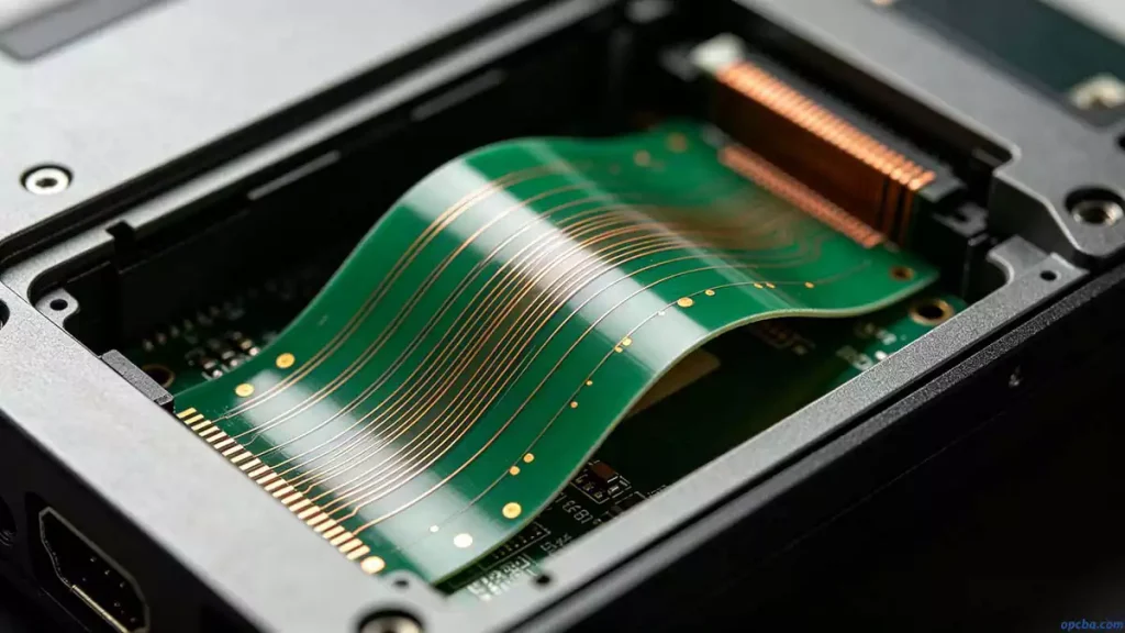
Semi-flex PCBs work by precision milling the bend area of a standard rigid FR4 board down to 0.25mm +/- 0.05mm.
This controlled thinning lets the board fold and mount cleanly into tight enclosures, and works for both single-bend fixed installations and multi-bend dynamic use cases.
What makes FR4 semi-flexible PCBs a practical choice
FR4 semi-flexible PCBs hit a sweet spot between performance and cost for most compact electronic designs, with core benefits that fit both consumer and industrial use cases:
- They bend to fit even the tightest enclosure spaces, with no drop in signal integrity through the flex zone
- Thin, lightweight construction cuts down overall product weight, a must-have for portable, wearable and handheld devices
- They run on standard rigid PCB fabrication lines, no specialized equipment needed, which keeps costs far lower than full rigid-flex builds
- Simplified design and assembly workflows cut down both development timelines and production lead times
- They eliminate the risks of loose wiring and hand soldering, delivering far more consistent long-term reliability than wired connections
How semi-flex PCBs are fabricated
The production flow follows standard rigid PCB processes for the most part, with one critical, high-control step: depth-controlled milling, which makes or breaks the board’s bending performance.
To better understand how PCB layer structure impacts milling accuracy and bend reliability, check out our detailed guide: PCB Layers Explained: Types, Functions & Differences in Altium Designer
We break the full workflow into logical production stages below:
Material prep and inner layer processing
- Material Cutting
- Dry film lamination
- Inner layer automated optical inspection (AOI)
Lamination and circuit formation
- Browning treatment
- Multi-layer lamination
- X-ray alignment inspection
- Through-hole drilling
- Copper electroplating
- Outer layer graphic transfer
- Circuit etching
Solder mask and surface finishing
- Solder mask screen printing
- Exposure and development
- Surface finish application (ENIG, HASL, etc.)
Flex zone forming and final inspection
- Depth control milling (core step for flex performance)
- Electrical continuity and isolation testing
- Final visual and dimensional quality control
- Vacuum-sealed packaging
Common production headaches and how to avoid them
In our daily fabrication work, the number one cause of semi-flex PCB failures is poor control during the depth milling process.
If the milling depth is off, you end up with resin cracking, solder mask flaking, or even the board snapping entirely when bent — all of which lead to scrapped parts and delayed production.
To avoid these issues, we strictly verify three core parameters before, during and after milling:
- Actual remaining board thickness in the designated bend zone
- Resin content uniformity in the layer being milled
- Milling depth and dimensional tolerances, matched to the design’s bend requirements
If you need reliable, high-yield fabrication for semi-flex PCBs, OPCBA has years of hands-on experience tuning this process for all kinds of compact designs.
Reach out to our team today to walk through your project requirements.


