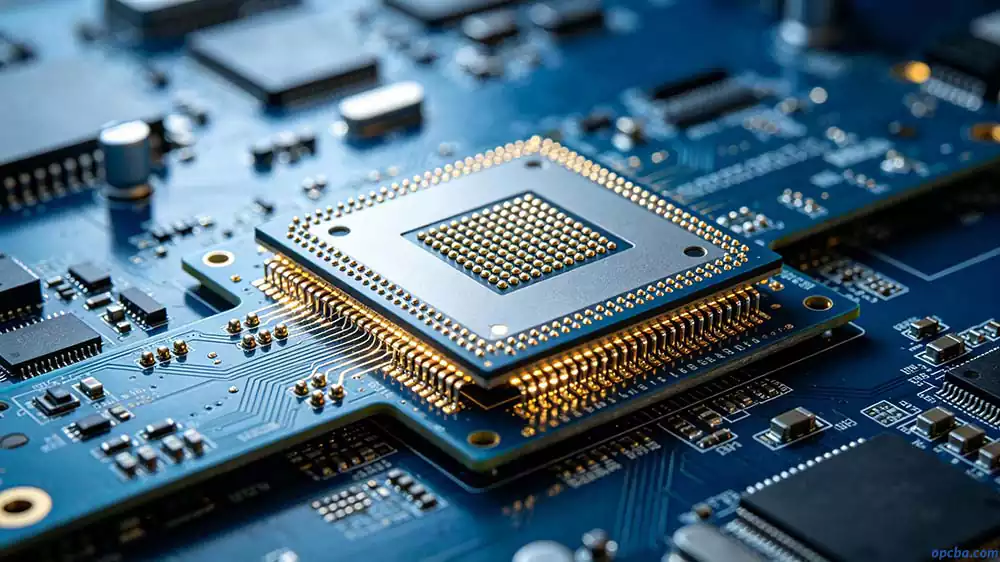
The moment a chip package moves beyond a few dozen pins, the old metal lead frame stops being practical. That’s where the IC carrier PCB takes over. It’s a high-density, multilayer board that sits between the silicon die and the main motherboard. It carries signals, power, and heat. I’ve seen designers treat the carrier as a black box. But understanding how it’s made and why certain formats win out helps. This is true when you’re selecting a package or troubleshooting a BGA-level failure. For more details on the product itself, see our page: IC Substrate
What the Substrate Actually Does (Beyond Holding the Chip)
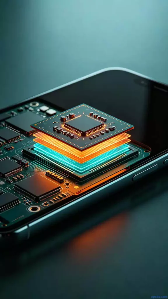
Think of the IC package substrate as more than a passive interposer. It provides a stable mechanical base for the die. It dissipates heat into the board. And it redistributes the fine-pitch C4 bumps to a coarser array of BGA balls. In many advanced designs, it also shelters embedded passives or even active components. This enables partial system-level integration before the chip ever reaches the motherboard. That “top and bottom” bridging role literally links chip to board. So the substrate’s layer count, material, and line width directly affect signal integrity and power delivery.
A Brief History: Three Phases of Change
The shift from lead frames to substrates happened in waves. Between 1989 and 1999, Japanese manufacturers dominated IC carrier PCB production. They established the early supply base for PBGA and CSP packages. Starting around 2000, Taiwan and South Korea scaled up their own IC package substrate capacity. This created a three-way split in global supply. The second phase saw volumes rise and costs drop, pushing substrates into consumer gear.
From 2004 onward, the game shifted again. Flip chip substrate demand exploded. High-end GPUs, CPUs, and chipsets drove this, needing dense bump arrays and tight line/space rules. MCM and SiP designs layered more functionality into the package. This turned the substrate into a compact system board in its own right. Today, Taiwanese and Korean firms hold most of the PBGA substrate volume. But Japanese suppliers still control a large share of the higher-margin flip-chip BGA and PGA substrates.
What Sets IC Substrate Manufacturing Apart
IC substrate manufacturing doesn’t work the way standard rigid PCB fabrication does. The typical line width and spacing fall in the 10–30 µm range. That’s well below what a conventional etch process can reliably hold. Modified semi-additive processing (mSAP) is the norm here. Thin copper seed layers are patterned and electrolytically built up to form fine traces. Meanwhile, dielectric layers use thin-core or coreless constructions to manage warpage and thickness.
Laser drilling handles microvias down to 40–60 µm. It enables stacked via structures that keep layer counts manageable. Surface finishes need to support wire bonding or flip-chip bumping. So you’ll see ENEPIG, soft gold, or OSP selected. Coplanarity specs are far tighter than on commodity boards. The imaging, etching, and lamination cycles are longer. Inspection steps multiply. AOI is run multiple times, often with 2D and 3D metrology on critical features. This is partly why a high-layer-count IC carrier PCB can cost orders of magnitude more than an equivalent FR4 board of the same layer count.
Flip-Chip and Beyond: Where It’s Heading
The continued push toward finer bump pitch keeps raising the bar on flip chip substrate technology. Pitches of 130 µm, 90 µm, and lower are now common. Coreless substrates with embedded passives are already standard in flagship smartphones. Chiplet architectures are encouraging large-format organic interposers. These blur the line between substrate and silicon interposer. Even glass-core substrates are emerging. But the fundamental challenge stays the same. How do you reliably connect thousands of die-level interconnects to a board-level array, without signal distortion or thermal cracking?
None of this is visible in a schematic symbol. But when a datasheet calls out an FC-BGA package, remember: the IC package substrate inside it was fabricated closer to semiconductor manufacturing than conventional PCB etching. For a designer, that means thermal vias, pad pitches, and keep-out zones are not arbitrary. They directly engage with what the IC substrate manufacturing process can deliver.


