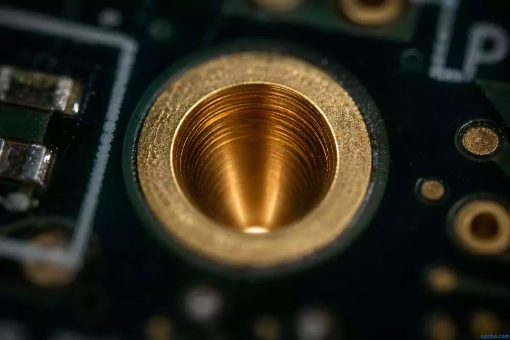
Plated vias are one of those PCB processes we use all the time—but they’re easy to overlook until something goes wrong. Put simply, it’s filling and sealing through holes with conductive metal plating, so those holes (which connect different circuit layers) work reliably.
The goal isn’t just to make the via conductive. By coating the inner wall with metal, we seal the hole completely—no gaps, no weak points. That small step makes a big difference in how the board holds up over time. For more details on PCB plating processes, check out our full guide: What Is PCB Side Plating? Types, Applications & Benefits
How Plated Vias Improve PCB Performance
We don’t use PCB plated via process for show—every benefit ties back to real-world performance, especially in dense or high-reliability boards.
For starters, sealed vias stop cross-layer short circuits. Nothing’s more frustrating than a board failing because a tiny gap in the via let two metal layers touch. Sealing them off cuts that risk way down.
They also make signal transmission cleaner. Filled vias minimize signal loss and impedance mismatch—issues that pop up with unplated or poorly plated holes. For high-speed circuits, this isn’t optional; it’s a must.
Soldering gets easier too. Plated vias create a flat, smooth surface, so solder adheres better. We see fewer cold joints and weaker connections when we use this process—saves time on rework later.
Structurally, filled vias make the board sturdier. They add rigidity, so the board holds up better to bending and vibration. Anyone who’s dealt with a cracked via mid-assembly knows how important that is.
And let’s not forget assembly. Uniform, sealed via surfaces make placing components easier—no uneven spots to throw off alignment. It speeds up the line and reduces component damage during mounting.
Potential Challenges of Plated Via Processing
As useful as they are, plated vias aren’t without headaches—we run into these issues all the time in production.
Cost is the first thing clients ask about. The extra materials (plating chemicals, filling compounds) and added steps push up manufacturing costs. It’s a trade-off between performance and budget.
Long-term reliability can be tricky too. Over time, thermal cycling, humidity, or corrosion can loosen the filling material or damage the plating. We’ve seen this happen with boards in harsh environments—something to factor into your design.
The process itself is pickier than standard via formation. You have to get hole preparation right, choose the right filling material, and nail the plating parameters. It takes better equipment and more skilled operators to keep things consistent.
There’s also extra work after filling. Larger vias need fillets to stay sealed, then we have to shave excess copper, grind, and polish to get a flat surface. That adds time to the production line.
And let’s not ignore the environmental side. Plating chemicals create wastewater and waste that needs proper treatment—you can’t just dump it. That adds another layer of complexity for compliance.
At the end of the day, plated vias are worth it for most high-reliability designs—but you have to weigh the pros and cons for your specific project. Get the process right, and you’ll avoid most of the headaches we’ve learned to anticipate.


