Description
1. What is PCB?
PCB is the English abbreviation for Printed Circuit Board, the industry is often called the bare board or bare board, is an important part of the electronic components of the support body, but also electronic components of the carrier of the electrical connection.
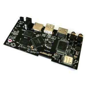
2. What is PCBA?
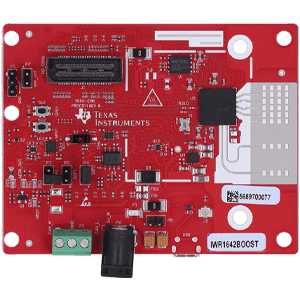
PCBA even if the PCB + component assembly, refers to the PCB board after the SMT on the pieces, and then after the DIP plug-in circuit board. Commonly known as the installation of resistors, integrated circuits, capacitors, and other components after the circuit board.
SMT and DIP are installed on the PCB board components, the main difference is that SMT does not need to drill holes in the PCB, while the DIP needs to insert the parts of the PIN foot that have been drilled in the hole.
SMT (Surface Mounted Technology) surface mount technology, the main use of the mounting machine is several micro-small parts mounted on the PCB board, the production process: PCB board positioning, printing solder paste, mounting machine mounting, over the soldering furnace, and making the inspection.
DIP that is, "plug-in", that is, in the PCB version of the insertion of parts, in which the size of some of the parts is large and does not apply to the mounting technology in the form of plug-in integrated parts. Its main production process is: paste the backing, plug-in, inspection, over the wave soldering, brush version, and made of inspection.
3. PCBA patch after the completion of commonly used test methods
(1) manual visual inspection
Artificial visual inspection is a more primitive method of PCBA test, mainly with the help of a magnifying glass to check the circuit of the PCBA board and electronic components of the welding situation, to see if there is a monument, even the bridge, more tin, weld whether the bridge, whether the welding is less welding and welding does not appear integrity. In today's PCB, the number of components and miniaturization trend is obvious, a lot of defects are difficult to find, and manual inspection is inefficient, not to make the PCB assembly line for mass production.
(2) AOI optical inspection
Automatic optical inspection, also known as automatic visual testing, is carried out by a specialized detector, used before and after reflow, the polarity of the components to check the effect is better. Optical inspection can not be completed on the physical aspects of the performance test, such as circuit on and off.
(3) ICT Needle Bed Test
In the mass production of factories, there is no way for you to use a meter to slowly measure each board on each resistor, capacitance, inductance, and even IC circuit is correct, so ICT (In-Circuit-Test) automated test machine, which uses multiple probes (generally referred to as the "Bed of Needles (Bed-Of-Nails)" fixtures) at the same time to contact the board on the All the parts that need to be measured line, and then by programmed to sequence-based, side-by-side as a complementary way to measure the characteristics of these electronic parts sequentially.
Needle bed to do circuit testing will have some limitations, for example: the minimum diameter of the probe has a certain limit, and too small a diameter of the needle is easy to break and destroy.
The distance between the needles also has a certain limit, because each needle has to come out of a hole, and the back end of each needle has to be welded to a flat cable, if the neighboring holes are too small, in addition to the needle and the needle will have contact between the short-circuit problem, the flat cable interference is also a major problem.
In addition, it is not possible to plant needles next to certain high parts. If the probe is too close to a high part, there is a risk of damage from collision with the high part. In addition, because the part is high, it is often necessary to cut a hole in the test fixture's needle bed holder to avoid it, which also indirectly makes it impossible to plant a needle. The circuit board is increasingly difficult to accommodate all the parts of the test point.
(4) Flying probe test
Flying probe test is considered by many to be a new test technology that is expected to replace the needle bed test, flying probe tester in the test accuracy, speed, reliability, coverage, and rapid progress in the past few years has been generally welcomed. In addition, for prototype (Prototype) manufacturing, small and medium production PCBs and PCBAs need to have a rapid changeover, and no fixture capacity of the test system requirements, so that the flying probe test flexibility and economic foot highlights.
The main advantages of a flying probe tester are that it can accelerate the time-to-market (time-to-market) tools, automatic test generation, no fixture costs, good diagnostics, and easy programming. Advanced flying probe testers also integrate 3D laser testing, burn-in programming, boundary-scan, and many other real functions.
(5) MDA manufacturing defect analyzer
MDA (manufacturing defect analyzer) is a tool for high-volume/low-mix environments, where testing is only used to diagnose manufacturing defects. Repeatability between testers is an issue when residual reduction techniques are not used. Also, MDA does not have a digital driver, so it cannot functionally test components or program on-board firmware (firmware). Test time is less than visual testing, so MDAs can keep up with the pace of the production line.
PCBA manufacturing process is complex, in the production process, may encounter a variety of product defects in the process. PCBA test methods and test equipment should be based on the specific characteristics of the PCBA to decide.
4. PCBA finished product testing
PCBA test is the most critical quality control link in the whole PCBA processing process, which determines the final performance of the product. Currently, the main test items of CBA include the ICT test, FCT test, aging test, and fatigue test.
ICT test: It mainly includes circuit breakage, voltage and current values fluctuation curves, amplitude, noise, and so on.
FCT test: IC program burning is required to simulate the function of the whole PCBA board, to find out the problems in hardware and software, and to equip with necessary production fixtures and test racks for SMD processing.
Aging test: mainly PCBA boards and electronic products for a long time to power, keep them working, and observe whether there is any failure failure, after the aging test of electronic products to batch factory sales.
Fatigue test: mainly on the PCBA board sampling, and function of high-frequency, long-time operation, to observe whether there is a failure, to determine the probability of failure of the test, and to provide feedback on the performance of the PCBA board within the electronic products.
5. PCBA simple processing technology flow:
(1) PCBA processing single-sided surface assembly process: solder paste printing - patch - reflow soldering;
(2) PCBA processing double-sided surface assembly process: A-side printing solder paste - patch - reflow soldering - flip-flop - B-side printing solder paste - patch - reflow soldering;
(3) PCBA processing single-sided mixed assembly (SMD and THC on the same side): solder paste printing - SMD - reflow soldering - manual insertion (THC) - wave soldering;
(4) Single-sided mixed device (SMD and THC are on both sides of the PCB): B-side printing red glue - patch - red glue curing - flip-flop - A-side plug-in - B-side wave soldering;
(5) double-sided mixing device (THC on side A, SMD on both sides A and B): A side of the printed solder paste - patch - reflow soldering - turn over the board - B side of the printed red glue - patch - red glue Curing - flip-flop - A-side insertion - B-side wave soldering;
(6) Double-sided mixed assembly (A and B sides both have SMD and THC): A side of the printed solder paste - patch - reflow soldering - turn the plate - B side of the printed red glue - patch - red glue cured -Flipboard -Side A insertion -Side B wave soldering -Side B insertion attached.
Soldering process, the smallest variables should belong to the machine and equipment, so the first check them, to achieve the correctness of the inspection, can be used for independent electronic negotiator assistance, such as using a thermometer to detect the temperature of the various, with a meter to accurately calibrate the parameters of the machine.
PCBA is an empty PCB through a process of processing and finally processed into a user-friendly electronic product. In the production process, a ring to a ring, whose link has a quality problem, will have a great impact on the quality of the product.
Contact OPCBA.COM to customize your digital products' PCBA.

分享到: