Description
1. What is an IC Substrate?
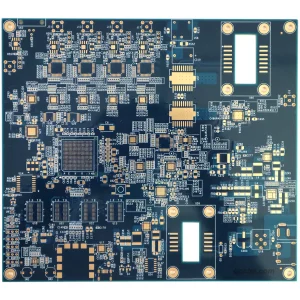
IC Substrate is a substrate used to encapsulate a bare IC (Integrated Circuit) chip. Connecting the chip and the board, IC belongs to the intermediate products with the following functions:
(1) Capturing semiconductor IC chips.
(2) Connecting chips and PCBs with internal wiring; and
(3) Protecting, reinforcing and supporting the IC chip, and providing heat dissipation tunnels.
2. Classification
(1) Classification by package type
– BGA IC Substrate. This type of IC Substrate performs well in terms of thermal and electrical performance and can significantly increase the chip pins. Therefore, it is suitable for IC packages with more than 300 pins.
– CSP IC Substrate. CSP is a single-chip package that is lightweight and small, with dimensions similar to those of ICs. CSP IC Substrates are mainly used for memory products, telecommunication products and electronic products with a small number of pins.
– FC IC Substrate. FC (Flip Chip) is a flip chip package with low signal interference, low circuit loss, good performance and efficient heat dissipation.
– MCM IC Substrate. MCM is an abbreviated form of Multi-Chip Module. This type of IC substrate absorbs chips with different functions into a single package. Therefore, this product can be the best solution due to its characteristics including lightness, thinness, shortness and miniaturization. Since multiple chips are encapsulated in one package, this type of substrate performs poorly in terms of signal interference, heat dissipation, and fine wiring.
(2) Classification by Material Properties
– Rigid IC substrate. It is mainly made of epoxy resin, BT resin or ABF resin. Its CTE (coefficient of thermal expansion) is about 13 to 17 ppm/°C.
– Flex IC substrate. It is mainly made of PI or PE resin and has a CTE of 13 to 27 ppm/°C – Ceramic IC Substrates. It is mainly made of ceramic materials such as alumina, aluminum nitride or silicon carbide. It has a relatively low CTE of about 6 to 8 ppm/°C.
(3) Classification by bonding technology
– Leaded Bonding
– TAB (Keyboard Auto Bonding)
– FC bonding
3. Applications
IC Substrate PCB is mainly used in light weight, light weight and powerful electronic products such as smart phones, laptops, tablets and networks in telecommunication, medical, industrial control, aerospace and military fields.
4. What’s the difference between SIP and SOC?
SIP is a single standard package that prioritizes the assembly of multiple active electronic components with different functions, with optional passive components, and other devices such as MEMS or optical devices, to achieve a certain function, forming a system or subsystem. Architecturally, SIP is the integration of multiple functional chips, including processors, memories, and other functional chips, into a single package to realize a complete function.
Soc refers to the integration of ICs with different functions into a single chip. Through this method, not only can reduce the size, but also can reduce the distance between different ICs, and enhance the chip’s computational speed. soc is called system-on-chip, also known as system-on-chip, which means that it is a product, is an integrated circuit with a dedicated target, which contains a complete system and embedded software in its entirety. At the same time it is a technology to realize the whole process starting from determining the system function to dividing the software/hardware and completing the design.
Since the development of IC device packaging from the development of individual components to the integration of multiple components, with the improvement of product performance and the demand for thin and light and low power consumption, led to a new stage of packaging integration. Under the guidance of this development direction, the formation of the electronics industry related to the two new mainstream: system-on-chip SOC (System on Chip) and systematic packaging SIP (System in a Package).
SOC and SIP are extremely similar in that both integrate a system containing logic components, memory components, and even passive components into a single unit.
SOC is from a design standpoint, where the components required for a system are highly integrated into a single chip. SIP is a side-by-side or stacked packaging of different chips from the standpoint of packaging, where multiple active electronic components with different functions are preferentially assembled with optional passive devices, and other devices such as MEMS or optical devices, to realize a single standard package for a certain function. The elements that make up SIP technology are the package carrier and the assembly process, the former including PCB, LTCC, Silicon Submount (which itself can also be an IC), the latter including traditional packaging processes (Wire bond and Flip Chip) and SMT equipment. Passive components are an important part of SIP, such as traditional capacitors, resistors, inductors, etc. Some of them can be integrated with the carrier, while others, such as inductors and capacitors with high precision, high Q, and high value, are assembled on the carrier through SMT.
In terms of integration, in general, SOC only integrates AP and other logic systems, while SIP integrates AP+mobileD DR, to some extent, SIP=SOC+DDR, with the increasing integration in the future, emmc is also likely to be integrated into SIP. From the perspective of packaging development, SOC was once established as the key and development direction of future electronic product design due to the demand of electronic products in terms of volume, processing speed or electrical characteristics. However, in recent years, the production cost of SOC has become higher and higher, and frequently encountered technical obstacles, resulting in the development of SOC facing a bottleneck, which in turn makes the development of SIP more and more important to the industry.