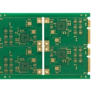
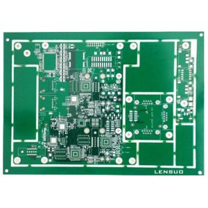
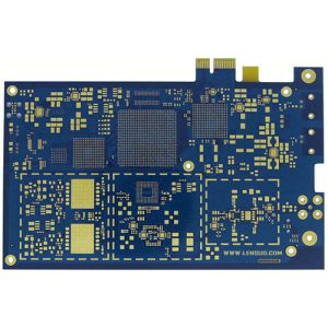
Description
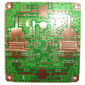
2 Layers PCB also called double-sided printed circuit board. A double-sided circuit board is a base material used for electronic circuit connection and assembly, consisting of two layers of printed circuit boards covered together at the top and bottom, interconnected by a different process that runs a conductive path between the two layers. This type of circuit board can provide higher line density and more complex circuit design and is a common component in electronic products.
1. Double-sided circuit board production process flow
Generally speaking, the process flow of single-sided circuit boards mainly includes: material grinding → drilling → outer layer of graphics → (full-board gold plating) → etching → inspection → silkscreen solder resist → (hot air leveling) → silkscreen characters → shape processing → test → inspection.
Double-sided circuit boards according to different materials and processes will be slightly different:
For example, the double-sided circuit board tin spray board process generally includes: material grinding → drilling → immersion copper thickening → outer graphics → tin plating, etching and retaining → secondary drilling → inspection → silk screen solder masking → gold-plated plug → hot air leveling → silk screen characters → shape processing → test → inspection.
Double-sided circuit board nickel gold-plated process flow generally includes: material grinding → drilling → immersion copper thickening → outer graphics → nickel plating, gold de-epitaxial etching → secondary drilling → inspection → silk screen solder resist → silk screen characters → shape processing → test → inspection.
According to the different processes, there will be different production processes, such as the graphic plating process, hole plugging SMOBC method and graphic plating method, and then back to the lead-tin SMOBC process of the two production processes are different. ps. SMOBC refers to the bare copper overlay solder mask process.
SMOBC process: double-sided copper-clad boards → etching process according to the graphic plating method → lead and tin withdrawal → inspection → cleaning → solder mask graphics → plug nickel and gold plating → plug tape → hot air leveling → cleaning → screen printing marking symbols → shape processing → cleaning and drying → product inspection → packaging → product.
SMOBC process flow of graphic plating and then retiring lead and tin: Double-sided copper-clad board → etching process according to the graphic plating method → retiring lead and tin → inspection → cleaning → solder masking graphic → plug nickel-gold-plated → plug taped → hot-air leveling → cleaning → screen-printed marking symbols → shape processing → cleaning and drying → product inspection → packaging → product
The process flow of graphic plating: Foil-covered board → Unloading → Punching and drilling of reference holes → Inspection → Deburring → Chemical thin copper plating → Inspection → Brushing → Film application → Exposure and development → Inspection and repair of the board → Plug nickel-plating and gold plating → Thermal fusion cleaning → Electrical on/off detection → Cleaning → Screen-printing of soldermask graphic → Curing → Screen-printing of marking symbols → Curing → Graphic Processing → Cleaning and drying → Inspection → Packaging → Finished products.
2. The production process of double-sided circuit boards mainly includes the following steps
(1) Cutting: Cut the circuit board into an appropriate size.
(2) Drilling: Use a CNC drilling machine to drill holes to ensure the accuracy of the holes.
(3) Plating and cladding process (PTH): the entire wall of the hole is plated with metal to realize the electrical interconnection between the inner and outer layers of the circuit board.
(4) screen printing: the use of specialized printing materials, copper-clad circuit boards printed on the line graphics, solder resist graphics, and character marking graphics.
(5) Tin-lead alloy plating: as a corrosion protection layer when etching and finished board solderability plating.
(6) etching: the unwanted copper etching off, to get the desired line.
After the completion of the above steps, the double-sided circuit board is completed. The specific process may vary depending on the production equipment and requirements. There are many other steps and details in the production process of double-sided circuit boards, the following are some additional production processes:
(1) Pre-treatment: Before the circuit boards are made, the copper-clad boards need to be pre-treated with cleaning, roughening, and activation to ensure that the subsequent processes are carried out smoothly.
(2) Graphics transfer: the designed circuit graphics are transferred to the copper-clad board, usually using photolithography or screen printing and other methods.
(3) graphic plating: the surface of the board is coated with a layer of metal to enhance the conductive properties and mechanical strength of the board.
(4) Retreated in cleaning: After the completion of plating, it is necessary to remove excess tin-lead alloy and cleaning treatment.
(5) Solder Resist Treatment: Solder resist is coated on the circuit board to prevent problems such as short circuits or leakage during the soldering process.
(6) Silk-screen marking: Print markings on the circuit board to facilitate assembly and maintenance.
3. Precautions for double-sided circuit boards
The fabrication of double-sided PCB boards is a complex and rigorous process that requires multiple steps and strict operating practices to ensure their quality and stability. During the production of double-sided circuit boards, the following matters need to be noted:
(1) The layout of the circuit board should be reasonable, to avoid too dense components or too complex wiring to ensure the electrical performance and mechanical stability of the circuit board.
(2) In the drilling process, ensure that the positional accuracy of the hole and the size of the hole, so as not to affect the connection performance and reliability of the circuit board.
(3) In the plating and etching process, the composition of the solution and process parameters need to be strictly controlled to ensure the quality of the circuit board plating and lines.
(4) In the welding process, it is necessary to avoid excessive heating or welding for too long to avoid damage to the circuit board or components.
(5) In the process of use, to avoid mechanical damage or chemical corrosion of the circuit board to ensure its long-term performance and reliability.
(6) In the manufacturing process, double-sided circuit board production needs to strictly comply with the relevant process specifications and operational requirements to ensure the quality and reliability of the circuit board.
Contact OPCBA.COM to get the information about 2 layers PCB.
分享到: