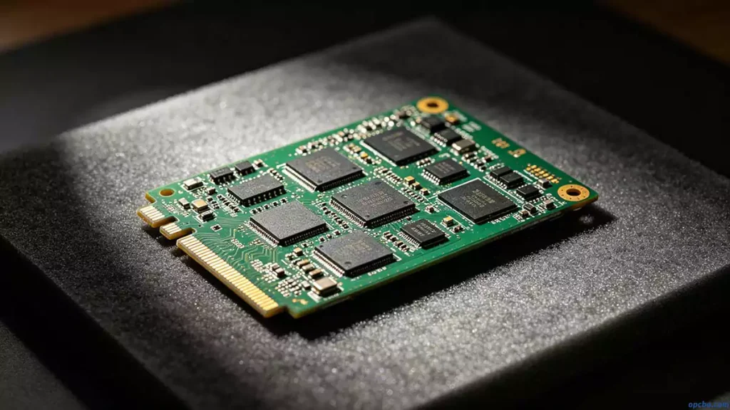
As electronics grow more advanced, assembly standards for printed circuit board assembly keep rising.
The overall reliability of any electronic device ultimately comes down to the quality of its PCBA. For a full introduction to this core process, check out our cornerstone guide: PCB Assembly(PCBA).
From our daily failure analysis work, one issue stands out clearly: leftover residues on the board directly weaken long-term stability.
Many manufacturers overlook this, but the impact is significant once boards enter real-world use.
Inorganic residues lower insulation resistance and raise leakage current between traces or solder joints.
In humid conditions, they also accelerate metal corrosion over time.
Organic residues like rosin and grease create insulating layers that disrupt contact in connectors, switches and relays.
These problems grow worse with age and environmental changes, often leading to intermittent connectivity faults or short circuits.
Testing Steps We Actually Use in PCBA Production
Testing is baked into every stage of PCBA manufacturing — it’s how we confirm components are placed correctly and function as intended.
Most factories use a mix of fixtures and tools to cover different inspection needs.
300X Microscope Inspection
This is our first-line visual check for quick, detailed analysis.
Set the board on the stage, adjust magnification and focus for a clear image, then rotate the lens 360° to examine all angles.
It helps identify cold joints, voids, foreign debris, solder balls, component damage, and solder fillet height on parts.
Red Ink Penetration Test
This test reveals hidden cracks and insufficient solder bonds that microscopes can miss.
Clean residual flux with 336A cleaner first, then apply red ink evenly across the target area.
Once the ink fully soaks in, bake the sample in an oven, then gently separate components with pliers.
We then examine the sample under a 300X microscope to spot stained gaps or fractures.
Cross-Section Slicing
For deep analysis of internal solder joint structure, we rely on slicing.
Mix acrylic powder and hardener at a 1:1 ratio, pour into a mold, and let it cure for 30 minutes.
After curing, grind the sample down to the defective area for close inspection.
This method works for checking cracks, voids, cold joints, and bonding quality on component leads.
Other routine tests include side microscopy, X‑RAY, solder paste inspection (SPI), and ongoing reliability testing (ORT).
How to Remove Contaminants From PCBA
Cleaning method depends entirely on batch size and required cleanliness level.
Manual Cleaning
Best for small batches or prototype boards.
We use a blend of anhydrous ethanol and isopropyl alcohol as the cleaning solution.
Dip a brush into the solvent and gently scrub solder joints to remove flux and debris.
Simple but effective for low-volume work.
Ultrasonic Cleaning
Used for medium-to-large batch processing with dedicated cleaning agents.
Boards go into a basket and soak in heated Freon for 4 minutes, then move to a cooling tank for ultrasonic cleaning.
After lifting the basket, we hold it above the steam zone until condensation stops, then air-dry for 15 minutes.
Water-Based Cleaning
Delivers the most consistent results and meets strict ionic contamination standards for military and high-reliability electronics.
The process uses a PBT-800P water cleaning machine with cleaning agent and deionized water.
Boards are loaded onto a moving rack, where high-pressure sprays handle cleaning, rinsing and drying automatically.
Final Notes for Printed Wiring Assembly
Small details like residue control, thorough testing and proper cleaning define the durability of printed wiring assembly.
These steps don’t just improve quality — they prevent early failures in the field.
Whether running prototypes or mass production, getting these basics right ensures your PCBA performs reliably under real operating conditions.


