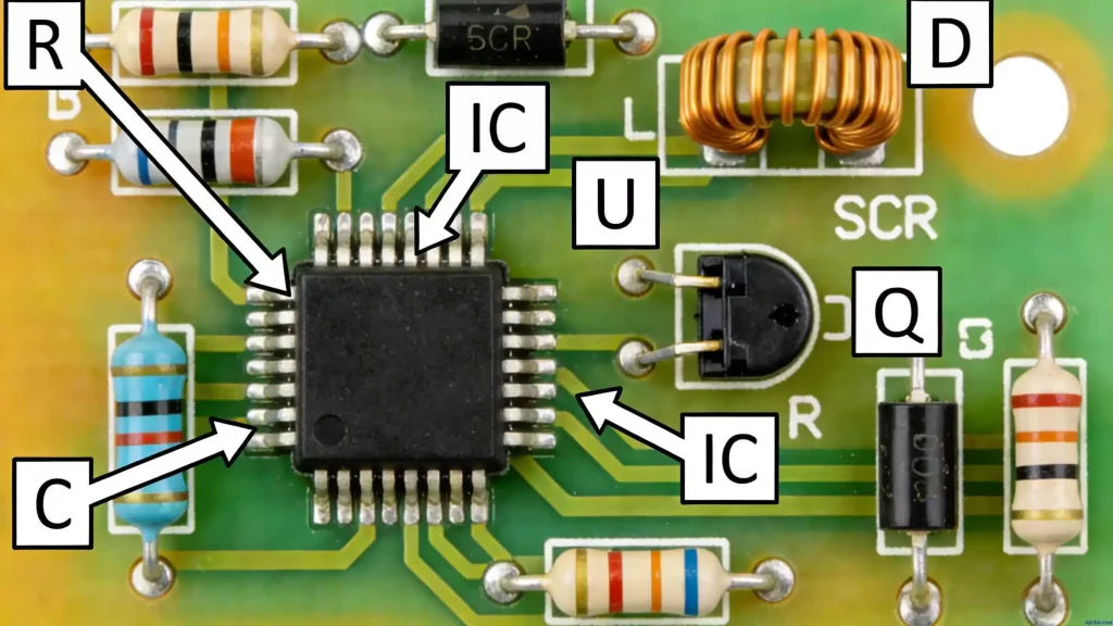
For PCB designers, especially those new to the field, understanding the different layers of a printed circuit board (PCB) is critical to creating reliable, manufacturable designs. When working in Altium Designer, each layer serves a unique purpose—from electrical connections to mechanical constraints. Keep in mind that while we focus on signal layers here, inner layers dedicated to power (plane layers) are also copper—they just serve a different purpose. Let’s break down the key differences between PCB layers and their roles in the design process.
1. Signal Layer (Top & Bottom)
Starting with the most essential layer for electrical functionality: the Signal Layer. These layers are the backbone of any PCB, carrying electrical signals between components to make your design work. In Altium Designer, single or double-sided boards use Top Layer and Bottom Layer, while multi-layer designs add internal signal layers—so don’t assume only signal layers contain conductive copper.
These conductive (typically copper) layers are used to:
- Place surface-mount and through-hole components
- Route electrical connections between component pins
- Support high-speed signal integrity in complex designs
Unlike non-conductive layers (like mechanical or silk screen), signal layers directly impact your board’s electrical performance. For high-power or high-heat designs, materials like Aluminum PCB can enhance thermal management, complementing careful routing and layer stacking to ensure reliability.
2. Mechanical Layer
Moving from electrical to physical: Mechanical Layers define your PCB’s physical form and manufacturing constraints, with zero electrical properties. Contrary to older information, modern Altium Designer versions (AD20 and later) support a very high number of mechanical layers (up to 1024), allowing for detailed fabrication and assembly documentation. Designers typically use a few key layers for the board outline, dimensions, and assembly notes—no need to overcomplicate it with dozens of layers.
These layers serve a range of non-electrical purposes:
- Sketching the board outline and edge cuts
- Defining mounting holes, keep-out zones, and component placement constraints
- Adding mechanical notes, assembly instructions, or manufacturing tolerances
For example, you might use one mechanical layer for the board outline and another for mounting hole dimensions—this keeps your design organized and easy for manufacturers to follow. Since these layers don’t affect electrical performance, you can add detailed notes or tolerances without worrying about short circuits or signal issues.
3. Silk Screen Layer (Top & Bottom Overlay)
Next up: the Silk Screen Layer (split into Top Overlay and Bottom Overlay), which is all about clarity for assembly and troubleshooting. Printed in white ink over the solder mask, this layer adds visual markers that make your PCB easier to work with—especially for beginners or technicians assembling boards by hand.
Common elements on the silk screen layer include:
- Component designators (e.g., R1, C2) and symbols
- Pin 1 markers for integrated circuits
- Test points, assembly notes, and copyright information
A common beginner mistake here is using tiny text for component designators (like R1 or C2)—if the text is too small, it’ll be unreadable after manufacturing. This layer isn’t just “decorative”; it’s what guides technicians to place components correctly and troubleshoot issues down the line.
4. Solder Paste Layer (Top & Bottom)
If you’re working with surface-mount components (SMDs), the Solder Paste Layer is non-negotiable. Split into Top and Bottom Solder Paste layers, this layer defines exactly where solder paste will be applied to component pads during assembly—think of it as a “stencil guide” for manufacturing.
Its key uses include:
- Create stencils for screen-printing solder paste onto pads
- Guide pick-and-place machines for accurate component placement
- Support reflow soldering processes
Unlike the solder mask layer (which covers copper), the solder paste layer only exposes pad areas. This precision ensures solder is applied exactly where it’s needed, reducing the risk of solder bridges (tiny connections between pads that cause short circuits)—a common issue in dense PCB designs.
5. Solder Mask Layer (Top & Bottom)
You’ve probably noticed most PCBs are green—that’s the Solder Mask Layer (Top and Bottom). Its primary job isn’t just to look good or protect copper (that’s what surface finishes like HASL or ENIG are for); its critical role is to prevent solder bridges between those tiny, closely spaced pads during assembly.
Its key functions include:
- Preventing short circuits from excess solder between adjacent pads during soldering
- Protecting copper traces from contamination and minor oxidation
- Reducing signal interference by isolating conductive paths
When you “open a window” in the solder mask layer, you’re exposing copper pads for soldering—that’s why pads look like shiny metal on finished PCBs. For test points or connectors, you’ll want to open these windows to ensure reliable soldering and easy access for debugging.
6. Drill Layer (Drill Guide & Drill Drawing)
While not the most “glamorous” layer, the Drill Layer is critical for manufacturing—without it, your PCB’s holes (for pads, through-holes, and vias) won’t be drilled correctly. This layer has two key parts, each serving a specific purpose:
- Drill Guide: A visual reference for hole locations and sizes
- Drill Drawing: A detailed manufacturing document with hole dimensions, tolerances, and plating requirements
Skipping or rushing the Drill Layer can lead to costly mistakes—for example, a misaligned hole could make a through-hole component impossible to solder. Taking time to double-check drill dimensions and locations here saves headaches during manufacturing.
7. Keep-Out Layer
The Keep-Out Layer is often misunderstood, especially by beginners. It defines boundaries where you can’t route signals or place components—but there’s a catch for modern designs.
When you draw a keep-out zone in Altium Designer, the software automatically restricts:
- Signal routing from crossing the zone
- Component placement within the zone
This layer was once the go-to for defining board boundaries, but it’s now considered a legacy feature (meaning you’ll mainly encounter it in older projects, but for new designs, there’s a better way). *Note: For modern designs, it is recommended to use a dedicated mechanical layer (e.g., Mechanical 1) to define the physical board shape and placement boundaries, and then set electrical clearance rules accordingly. The Keep-Out Layer is retained for legacy project compatibility.* This approach is more flexible and aligns with modern Altium design workflows.
8. Multilayer
Last but not least: the Multilayer, an abstract layer in Altium Designer that acts as a “bridge” between all conductive layers. Pads and vias (which go through the entire board) are assigned to this layer by default—they need to connect to multiple signal layers, so the Multilayer ensures they’re visible and functional across the entire PCB.
A quick pro tip: If you’re troubleshooting layer visibility, try toggling the Multilayer on/off. Disabling it hides pads and vias, which can help you focus on specific signal layers without clutter—handy for checking routing or layer stacking issues.
Pro-Tips for Working with PCB Layers in Altium Designer
To tie everything together, here are actionable tips to use these layers effectively in real projects—no fluff, just practical advice:
- Name your layers clearly: Use descriptive names (e.g., “Mechanical 1 – Board Outline” instead of “Mechanical 1”) to avoid confusion, especially when collaborating.
- Don’t overcomplicate mechanical layers: Stick to 2-3 key mechanical layers (outline, dimensions, notes) to keep your design clean and manufacturable.
- Test silk screen readability: Zoom out to 1:1 scale in Altium to check if component designators are readable—if they’re too small, increase the font size.
- Prioritize solder mask windows: Always double-check that pads, test points, and connectors have solder mask windows open—missing windows mean you can’t solder components.
- Embrace modern workflows: Ditch the Keep-Out Layer for mechanical layers + design rules—it’s more flexible and aligns with how manufacturers work today.


