PCB copper plating quality directly impacts the board’s application reliability. As PCBs move toward higher density and precision, demands for plating quality keep rising—coating must be uniform, fine, and free of PCB copper plating defects like pits, pinholes, and incomplete copper coverage. To learn more about related copper exposure issues in PCB manufacturing, check out our guide: How Does Exposed Copper on PCBs Occur? Design and Manufacturing Details You May Have Overlooked
At our institute, PCB copper plating pits were once the top issue affecting plating surface quality. We focused on two key production processes—graphic transfer and graphic electroplating—to optimize parameters and tighten control, cutting pit occurrence and ensuring plating quality.
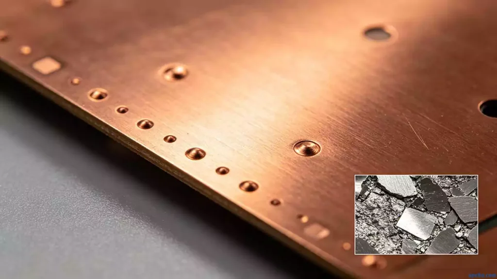
What Do Copper Plating Pits Look Like?
Copper plating pits are dotted depressions on large copper surfaces, circuits, and pads after graphic copper plating. They’re most commonly found along circuit or pad edges (see Figure 1).
Metallographic sections of these pits (Figure 2) show incomplete copper plating—some areas even have no copper at all.
Figure 1: Copper Plating Pit | Figure 2: Metallographic Section of Copper Plating Pit
Cause Analysis & Control Measures
We mapped the root causes of copper plating pits using a fault tree (Figure 3)—most issues trace back to graphic transfer or post-development storage.
Figure 3: Fault Tree of Copper Plating Pits
Graphic Transfer Process Issues
Graphic transfer moves circuit images from photographic plates to copper-clad laminates, forming an etching or electroplating-resistant mask. The process includes board brushing, film lamination, exposure, and development—each step can introduce pits if not controlled.
1. Board Brushing Effect
Board brushing removes surface oxidation and dirt. If the brushing machine fails to clean the board thoroughly, residues will inhibit copper plating and form PCB copper plating pits.
In our institute, we once faced frequent pit defects. Metallographic sections revealed foreign matter on the secondary copper, blocking further electroplating (Figure 4). The issue? Inappropriate abrasive brush roller mesh sizes (320-mesh first section, 500-mesh second section) and aging rollers.
We replaced the first section with 500-mesh rollers and the second with 800-mesh—and the pit defects disappeared entirely. Figure 4: Foreign Matter Causing Copper Plating Pits
2. Dry Film Residue During Exposure
Dry film residue in alignment tables or exposure machines (from alignment and exposure) adheres to the board surface, causing pits and even serious wire breaks (Figure 5) if not cleaned promptly.
We fixed this by implementing regular cleaning: before each shift, use electrostatic precipitator rolls to remove debris from alignment tables, exposure machines, and clamps. Wipe these areas with anhydrous alcohol-soaked paper, and clean exposure glass, Mylar film, and negatives at least every five exposures.
Figure 5: Wire Break Caused by Exposure Machine Debris
3. Development Effect
Water-soluble dry film developers use 1%~2% anhydrous sodium carbonate solution. Unexposed photosensitive film reacts with the alkali to form soluble colloids—dirty developer or improper parameters leave glue residues, leading to thin or no plating and pits.
We learned 1L of developer dissolves 0.25㎡ of dry film (or 0.3㎡ of PCB). Initially, we changed developer based on production cycles, but later tests linked processing area to pit probability (Table 1, Figure 6).
Figure 6 shows pit probability rises sharply when processing area exceeds 150㎡. We now change developer every 150㎡ processed. Monthly, we use special cleaners to deep-clean tank pipelines—regular alkaline/acid cleaning isn’t enough.
Table 1: Effect of Developer Processing Area on Copper Plating Pits | Figure 6: Processing Area vs. Pit Rate Trend
Storage Time Between Development & Electroplating
This window is critical. Exposed copper reacts with air (O2, CO2, moisture) over time, forming hard-to-remove oxide layers that cause pits during electroplating.
We once left boards unplated for up to 4 days after development—surface oxidation became unremovable, creating pits (Figure 7). Extended storage also lifts dry film, causing plating infiltration.
We now require this storage time to not exceed 48 hours. Figure 7: Copper Plating Pits From Extended Storage
Improvement Effect Tracking
After optimizing graphic transfer and electroplating parameters, we tracked scrap rates (Table 4). Double-sided board scrap rate dropped from 1.88% to 0.42%, and multilayer board scrap rate from 2.11% to 0.85%—a more than 3x reduction in pit-related scrap.
Key Takeaways
We analyzed PCB copper plating pits from graphic transfer and electroplating perspectives, implementing targeted improvements that cut scrap rates significantly. The biggest lessons? Consistent solution maintenance, regular tank cleaning, and strict detail control—these small steps make all the difference in plating quality.


