Etching is the core manufacturing step that removes unwanted copper from circuit boards to form precise conductive patterns. It uses chemical reactions (wet etching for PCB) or plasma (dry etching) to dissolve unprotected metal, leaving only the desired traces, pads and planes.
At OPCBA, our PCB etching process has been refined through years of production experience to balance precision, efficiency and yield. This guide breaks down the complete workflow and critical points that separate high-quality results from common defects.
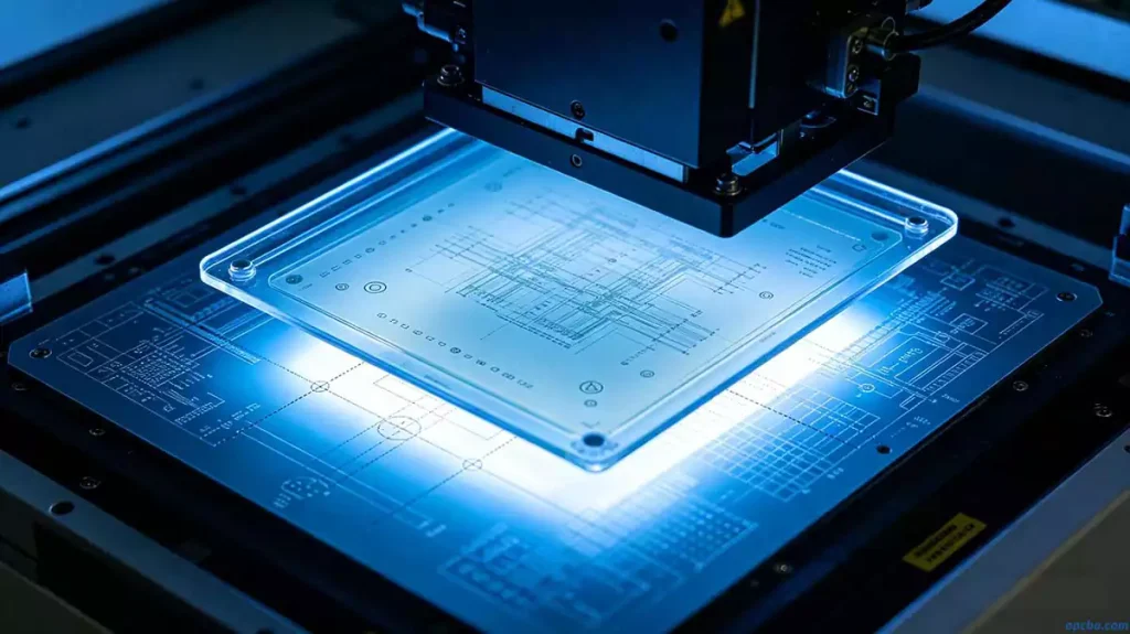
The Complete PCB Etching Workflow
1. Incoming Inspection (IQC)
Every batch starts with incoming quality control. We wipe down customer workpieces to remove surface contaminants, then inspect for defects like scratches, oxidation or warpage. In practice, even minor issues here can lead to etching problems later—so we catch them before they enter production.
2. Surface Preparation: Dust Removal & Photoresist Coating
Before applying photoresist, electrostatic dust removal is non-negotiable. Static builds up during handling and cleaning, attracting particles that ruin fine patterns. Our automated system neutralizes static and removes dust completely.
We then spray a uniform layer of liquid photoresist (or apply dry film) to both sides of the board. After coating, operators check for uneven coverage, missed spots or residue—common issues that cause under-etching or shorts.
3. Photolithography & Development
Photolithography transfers the circuit pattern from film to the photoresist-coated board. We position the film carefully over the workpiece; misalignment here creates pattern distortion, a top cause of rejects. Film condition matters too—creases or damage lead to defective patterns, so we inspect films regularly.
Development follows exposure: a chemical bath dissolves unexposed resist, leaving cured resist that protects the desired copper. Quality inspectors check for under-development (resist remains where it shouldn’t) or over-development (resist lifts where it should stay).
4. Edge Sealing (Oil Sealing)
This often-overlooked step prevents etching solution from seeping under the resist at board edges. Operators apply a special sealant manually to areas where spray coating might be thin. The key is full coverage without exposing copper—any gaps cause edge erosion defects.
5. Etching & Post-Process Cleaning
The heart of the PCB etching process uses a chemical solution (typically ammonium persulfate or cupric chloride) to dissolve exposed copper. We monitor temperature, concentration and agitation constantly—variations here affect etch rate and uniformity.
After etching, we remove residual resist with a stripping solution, then clean thoroughly with a slow-pull rinsing machine to eliminate chemical residues that cause reliability issues later.
6. Final Inspection (FQC)
Before shipment, every board undergoes final quality control. Inspectors check for proper trace definition, no shorts/open circuits, and uniform etching across the panel. First Article Inspection (FAI) is mandatory for new designs to verify the entire PCB etching process meets specifications.
Critical PCB Etching Precautions
Based on thousands of production runs, these are the non-negotiable practices for consistent results: To fully understand the technology and baseline standards that support these precautions, check out our guide: PCB Etching Technology and Basic Requirements
- Minimize side etching: Maintain proper etchant temperature (45-55°C) and agitation to control the etching coefficient—the ratio of vertical to horizontal copper removal
- Ensure uniformity: Rotate workpieces and maintain consistent solution concentration to prevent uneven etching across large panels
- Control thin copper etching: For 12-18μm copper, reduce etch time and monitor closely to avoid over-etching fine features
- Prevent contamination: Regularly filter etchant and replace when metal content exceeds 120g/L to maintain etching performance
- Safety first: Use PPE (gloves, goggles, aprons) and ensure proper ventilation—etching chemicals cause severe skin/eye irritation
Why These Steps Matter
In high-volume production, the PCB etching precautions we’ve outlined directly impact yield and cost. A 1% increase in first-pass yield saves thousands in rework and material waste. Our process balances speed with precision, supporting everything from simple single-layer boards to complex HDI designs with 0.05mm line/space requirements.
If you have questions about custom etching requirements, material compatibility or process optimization for your PCB project, contact OPCBA for expert technical support and manufacturing solutions.


