PCB potting is widely applied in electronic manufacturing to protect boards from moisture, dust and corrosion.
As product reliability demands keep rising, PCB potting has become a standard step in modern PCBA production.
Three types of PCB potting adhesive are most commonly used: polyurethane, silicone and epoxy resin.
Common Types of PCB Potting Adhesives
Polyurethane Potting Compound
This material cannot withstand temperatures over 100℃ and usually requires vacuum operation to reduce bubbles.
It offers moderate bonding strength, excellent low-temperature performance and the best shock resistance among the three.
In real production, it shows relatively poor toughness and an uneven surface after curing.
Chemical resistance is also limited, making it less ideal for harsh high-temperature environments.
Silicone Potting Compound
Silicone-based potting stands out for impact resistance, aging resistance and stable physical performance.
It maintains consistent properties under frequent thermal cycling and provides strong electrical insulation.
It also supports easy rework for component repair or replacement.
With low viscosity and good fluidity, it improves component heat dissipation and safety.
The main drawbacks are weaker adhesion, lower confidentiality and higher cost, suited for long-term harsh-environment electronics.
Epoxy Resin Potting Compound
Epoxy offers good heat resistance, strong electrical insulation and stable curing performance.
It bonds well to most metals and porous substrates, with simple operating requirements.
It performs poorly in low temperatures and can crack under thermal shock, which may damage components.
The cured material is hard and brittle, so it’s mainly used for electronics in stable room-temperature environments.
Why PCB Potting Adds Real Value to Electronics
PCB potting delivers long-term protection for sensitive circuits and components in high-demand applications.
It provides stable dielectric insulation, blocks environmental contaminants and reduces stress from vibration and temperature changes.
Most modern potting materials use condensation or addition curing systems with no need for secondary curing.
They can be formulated for thermal conductivity, flame retardancy and transparency, while curing evenly regardless of thickness.
Key Advantages of PCB Potting
- Excellent moistureproof and waterproof performance for long-term outdoor or harsh use
- No corrosion to metal parts, safe for PCB module potting
- Flexible gel structure with strong shock and deformation resistance
- High insulation ensures stable performance after potting
- Good self-leveling fluidity improves production efficiency
- Removable formula allows component repair, rework and resealing
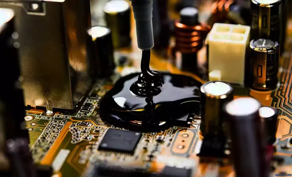
Practical PCB Potting Process
Follow this field-proven PCB potting process to ensure consistent, defect-free results.
- Clean the PCB thoroughly with anhydrous alcohol and a stiff brush, removing rosin, solder residue and debris.
- Dry the board with a hot-air tool and inspect for cold joints, short circuits or leftover solder slag.
- Apply a base waterproof coating by brushing or dipping the PCB, before or after wiring.
- Allow at least 12 hours for full curing; accelerated drying can be used for urgent orders.
- Test circuit function. If abnormal, remove the coating and repeat the coating step.
- Use epoxy, silicone or adhesive to fully pot the board inside the housing, eliminating air gaps.
- Let the potting cure for at least 24 hours, then perform random or full functional testing.
For more details about PCB potting solutions, feel free to inquire at opcba.com.


