If you work in the PCB industry, you’ve probably heard of burn-in board testing—but many professionals still mix up its purpose, process, and material needs.
PCB burn-in board testing is far more than a routine check. It’s a non-negotiable step to uncover hidden defects early, ensuring PCBs deliver consistent reliability, especially for high-stakes applications like medical devices or industrial controls.
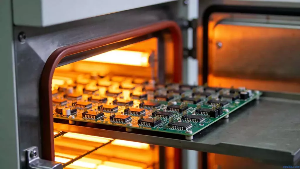
A burn-in board is a specialized loaded board built for high-temperature aging tests. When a circuit board runs for a set period under specific conditions, some component parameters may shift—tiny changes that can cause malfunctions down the line. That’s why most PCB makers add anti-aging treatment before shipment: it stabilizes the circuit before use, boosting overall reliability and safety.
What Exactly Is a PCB Burn-in Board?
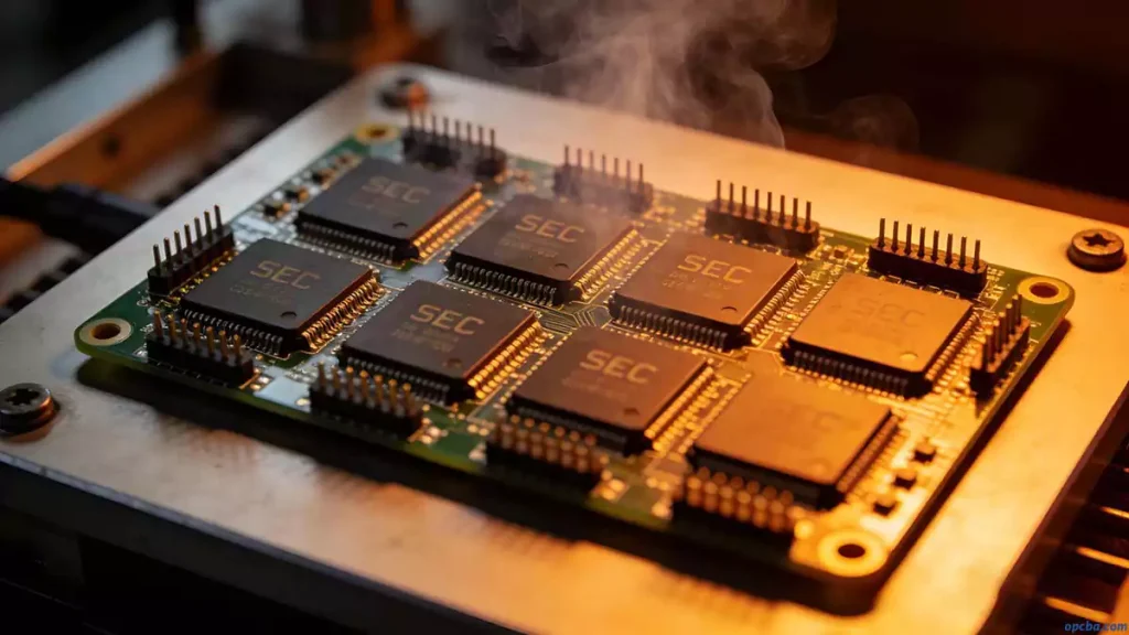
It’s not a standard PCB—PCB burn-in board is purpose-built for aging testing. These boards feature dedicated sockets to secure ICs (like ASICs) and other components, streamlining the testing process. To learn more about the foundational circuit board technology that burn-in boards are built on, check out our guide: Printed Circuit Board(PCB).
During testing, the burn-in board holds the sample ICs, and the entire setup goes into an aging furnace. The temperature stays fixed at 125°C (257°F)—a harsh condition that pushes components to their limits. This stress helps reveal latent defects, so faulty parts get culled before they reach end products.
How Does the Burn-in Test Work?
In real production, the test follows a strict temperature cycle, designed to mimic real-world usage and stress test vias and components:
- Start at -40°C, hold for 1 hour
- Warm to room temperature, maintain 4 hours
- Heat to 125°C, hold 2 hours
- Cool back to room temperature, hold 2 hours
- Repeat the full cycle twice for thorough validation
This cycle isn’t just a formality. It targets weak vias, faulty connections, and unstable components that regular inspections might miss. After testing, samples are screened to confirm they passed the oven test, ensuring the final PCB’s quality and functionality.
What Materials Are Used for Burn-in Boards?
Since burn-in boards endure extreme heat (up to 300°C in some tests), regular PCB materials won’t cut it. The choice hinges on the test temperature:
- Basic tests (≤125°C): High Tg FR4 (flame-retardant) — cost-effective and durable for standard aging tests
- Mid-range (up to 250°C): Polyimide materials — better heat resistance than FR4, no structural degradation
- High-temp (300°C+): High-quality polyimide — the only material that can withstand extreme heat without warping or failing
Why This Testing Matters
Burn-in testing is critical for applications where failure isn’t an option: aerospace electronics, medical implants, and industrial machinery all rely on it to meet safety and performance standards. Skipping this step often leads to costly recalls, product failures, or safety risks—something no PCB manufacturer can afford. For a full look at the next step in the production process after burn-in testing, explore our guide: PCB Assembly(PCBA).


