Printed circuit board (PCB) materials fall into two main categories: organic substrate materials and inorganic substrate materials, with organic substrates being the most widely used. Different PCB layer counts require distinct materials—for example, 3-4 layer boards often use prefabricated composites, while double-sided boards typically rely on glass-epoxy substrates like FR-4. PCBs are constructed from a combination of insulating/dielectric and conductive materials to form circuit interconnects, with a wide range of options available to balance performance, durability, and budget. Selecting the right PCB material is critical to ensuring the functionality and reliability of your final electronic device, requiring a clear understanding of material properties and how they align with your board’s intended use case.
1. PCB Material Categories Overview
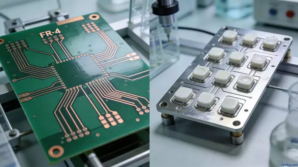
Organic substrate materials (e.g., FR-4, CEM-1, polyimide) dominate commercial PCB production due to their cost-effectiveness and balanced electrical/mechanical properties. Inorganic substrates (e.g., ceramic, metal-core PCBs) serve specialized high-temperature or high-thermal-conductivity applications. The choice between these categories depends on your PCB’s operating environment, assembly process, and performance goals.
2. Key Selection Factors for PCB Materials
2.1 Align with SMT Assembly Requirements
Lead-free electronic assembly exposes PCBs to higher temperatures, increasing thermal bending stress. To minimize warpage and component reliability risks, select low-bending substrates like FR-4. You must also prioritize materials with a controlled coefficient of thermal expansion (CTE), especially for components larger than 3.2×1.6mm—excessive expansion/contraction stress can cause electrode peeling and reduced device lifespan.
PCBs for surface mount technology (SMT) must meet strict performance standards:
- High thermal conductivity and excellent heat resistance (150°C for 60 minutes)
- Reliable solderability (260°C for 10 seconds)
- Strong copper foil adhesion (≥1.5×10⁴ Pa) and flexural strength (≥25×10⁴ Pa)
- Low dielectric constant and high electrical conductivity
- Precise blanking accuracy (±0.02mm) and compatibility with cleaning agents
- Smooth, warpage-free surface free of cracks, scars, or rust spots
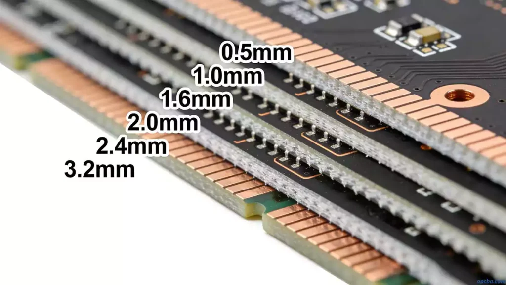
2.2 Meet PCB Thickness Requirements
Standard PCB thicknesses include 0.5mm, 0.7mm, 0.8mm, 1mm, 1.5mm, 1.6mm, 2.7mm, 3.2mm, 4.0mm, and 6.4mm. Non-standard sizes like 1.8mm and 3.0mm are less common and may limit manufacturing flexibility. For double-sided boards with gold fingers, 0.7mm and 1.5mm thicknesses are preferred.
From a production perspective, the minimum single PCB size should be no less than 250×200mm, with an ideal panel size of (250–350mm) × (200–250mm). PCBs with a long side <125mm or wide side <100mm require panelization to optimize manufacturing efficiency. For 1.6mm thick substrates used in SMT, the allowable warpage is ≤0.5mm (upward) and ≤1.2mm (downward), with a general acceptable bending rate below 0.065%.
2.3 Account for PCB Drilling Requirements
The rise of SMT and multilayer PCBs has made drilling a critical production step, as electrical connectivity between layers relies on plated through holes (PTHs). CNC mechanical drilling is the most common method today, with laser drilling used for ultra-fine pitch applications.
Hole processing accounts for a significant portion of PCB production time, and the positional accuracy and hole wall quality directly impact downstream processes like metallization and component placement—ultimately affecting the PCB’s final quality and cost. Modern CNC drilling machines are designed to meet the precision demands of high-density interconnect (HDI) PCBs and complex multilayer designs.
3. Critical PCB Material Properties (IPC 4101 Standard)
The IPC 4101 specification for rigid and multilayer PCB materials defines four core thermal properties that are essential for material selection:
3.1 CTE (Coefficient of Thermal Expansion)
CTE measures how much a material expands when heated, with the z-axis (through-thickness) expansion being most critical for multilayer PCBs. Expansion rates typically accelerate above the material’s glass transition temperature (Tg). Insufficient or excessive CTE can lead to assembly failures, as rapid thermal expansion above Tg stresses component solder joints and layer interconnects.
3.2 Tg (Glass Transition Temperature)
Tg is the temperature at which a PCB material transitions from a rigid, glassy state to a flexible, rubber-like state. Above Tg, the material’s expansion rate increases sharply. Two materials can have the same Tg but very different CTE values—lower CTE is always preferred for improved thermal reliability.
3.3 Td (Decomposition Temperature)
Td is the temperature at which a laminate material begins to decompose, releasing volatile components. Reliability is compromised when the material loses 5% of its original weight, leading to delamination and electrical failure. For high-reliability PCBs or those operating in demanding conditions, Td should be ≥340°C.
3.4 T260/T288 (Delamination Time at 260°C/280°C)
T260 and T288 measure the time it takes for a PCB laminate to delaminate at 260°C and 280°C, respectively. Delamination occurs when the epoxy resin matrix thermally decomposes, causing irreversible changes in PCB thickness and structural integrity. These metrics are critical for evaluating a material’s performance during lead-free soldering and high-temperature operation.
4. Final PCB Material Selection Best Practices
To choose the most suitable PCB material, align the laminate’s thermal and mechanical properties with your assembly process and operating environment. Prioritize materials that balance cost, performance, and reliability, and always reference IPC 4101 standards for critical applications. For complex projects, consult with PCB manufacturing experts to optimize material selection for your specific design needs.
For custom PCB material selection and manufacturing support, contact OPCBA for expert guidance tailored to your project requirements.


