PCB etching technology is a core process in PCB fabrication, used to create precise circuit patterns on copper-clad substrates. It leverages the photosensitivity of chemical photoresist materials to transfer accurate circuit designs onto the substrate, then uses pressurized etchant to remove unwanted copper, leaving behind the desired geometric circuit patterns with tight dimensional tolerances.
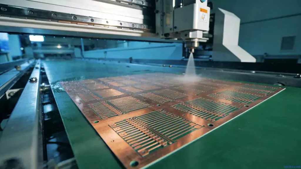
In practice, etching works by spraying etchant evenly across the copper foil surface at a controlled temperature. Unprotected copper (without etch-resistant mask) undergoes a redox reaction with the etchant, dissolving away to expose the base substrate. The remaining circuit pattern is then finished with resist stripping. Common etchant components include copper chloride, hydrogen peroxide, hydrochloric acid, and high-purity soft water with strict solubility controls.
Standard PCB Etching Process Flow
The core etching sequence follows three key steps: 1. Dry film stripping 2. Circuit pattern etching 3. Tin-lead resist stripping
Critical Quality Requirements for PCB Etching
Meeting consistent PCB etching process requirements is non-negotiable for defect-free PCB production. Below are field-proven control points and quality standards for high-volume manufacturing.
No Residual Copper or Resist
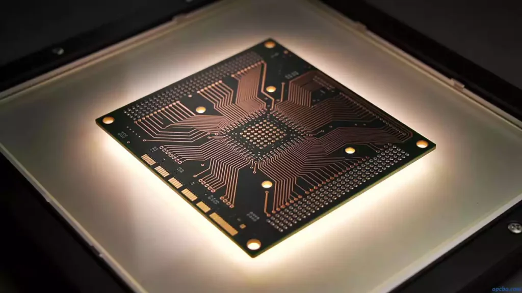
In real production, residual copper is one of the most frequent etching defects, especially on double-sided boards. No unetched copper should remain on the finished board, even in tight gaps between fine traces. Residual photoresist must also be fully removed, as leftover film will cause poor adhesion in subsequent plating or soldering processes.
Etching Uniformity & Line Width Control
Over-etching leads to trace thinning, which impacts electrical performance and can cause open circuits. Etching speed and etchant spray uniformity must be tightly controlled to avoid inconsistent etching across the board, whether between top/bottom sides or different areas of the same surface. For standard trace widths of 0.2mm and 0.25mm, the allowable etching tolerance is ±0.02mm.
Pattern & Surface Integrity
The dry film on component pads must not lift or break during etching, which would cause pad damage or short circuits. After resist stripping, the board must be free of oil, contaminants, or lifted copper foil. Traces must be free of deformation, wrinkles, scratches, oxidation, or water spots. 100% light transmission inspection is required to confirm no hidden copper residue remains.
Production Handling Best Practices
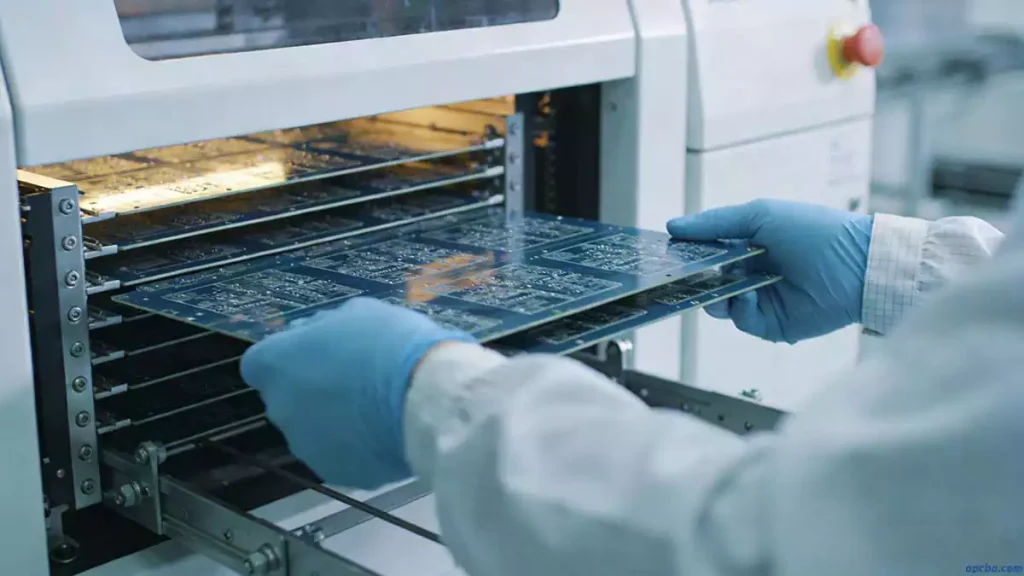
Boards must be loaded carefully to avoid jams in the etching machine, which can cause over-etching or physical damage. Proper handling also prevents post-etch oxidation, which will degrade the board’s solderability in later assembly steps.
PCB Etching Equipment
Consistent PCB etching quality control starts with well-maintained etching equipment. Modern etching machines use precision nozzle systems to deliver uniform etchant spray across the board surface, with tight controls for temperature, pressure, and conveyor speed. These variables directly impact etching consistency, trace dimensional accuracy, and overall defect rates. For a detailed guide on selecting and maintaining etching equipment, explore our dedicated resource: PCB Etching Equipment Selection Guide.
From prototype to high-volume production, mastering PCB etching technology is foundational to manufacturing reliable, high-performance PCBs. For more details about PCB etching equipment and full PCB fabrication services, visit opcba to discuss your project requirements.


