In high-speed circuit design, the inductance and capacitance within PCB traces turn wires into equivalent transmission lines. Poor placement of termination components or incorrect high-speed signal routing can trigger transmission line effects—leading to data errors, abnormal circuit behavior, or even full system failure. Using a transmission line model, engineers can identify risks like signal reflection, crosstalk, electromagnetic interference (EMI), and power/ground noise—challenges also central to RF antenna PCB design. Learn more about high-frequency signal integrity in our guide: RF Antenna Design and PCB Design. To create a reliable high-speed PROTEL PCB, designers must carefully address layout and wiring challenges, shorten product development cycles, and boost market competitiveness.
1. PCB Size & External Component Connection Basics
The design of a printed circuit board (PCB) starts with defining board dimensions, which are limited by the chassis shell size—so the board must fit neatly within the enclosure. Next, designers must consider how the PROTEL PCB connects to external components (such as potentiometers, sockets, or other PCBs). Most often, plastic or metal isolation wires link the PCB to external parts, but socket-based connections are also an option for larger designs. For heavy components mounted on the PROTEL PCB, add metal mounting brackets to improve vibration and impact resistance, ensuring long-term reliability.
2. Core Component Layout Principles for PROTEL PCB
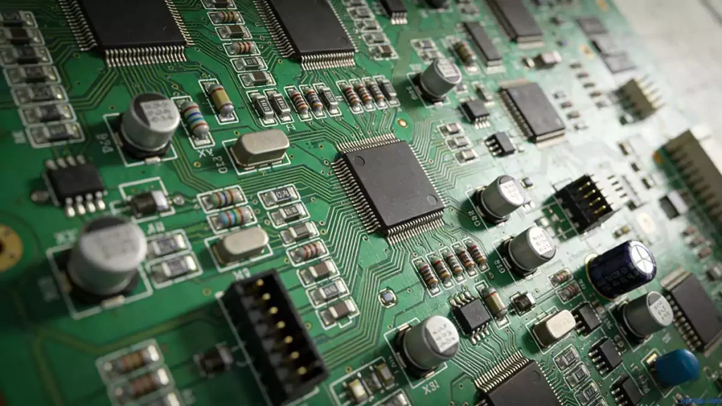
Effective PROTEL PCB layout begins with a thorough understanding of component specifications, dimensions, and pinouts. Designers must arrange components carefully, prioritizing electromagnetic compatibility (EMC), anti-interference performance, short trace lengths, minimal crossings, clear power/ground paths, and proper decoupling. Once component positions are finalized, the next step is to connect pins according to the schematic.
Manual vs. Computer-Aided Layout
Two primary methods exist for PROTEL PCB layout: manual and computer-aided design (CAD):
- Manual Layout: The most basic approach, where designers arrange components and traces by hand. This process is tedious and often requires multiple iterations, but it works without specialized CAD tools. It also serves as a valuable learning exercise for new PCB designers, helping them master core layout principles.
- CAD Layout: Modern PROTEL PCB design relies on CAD software, which offers convenient drawing, editing, saving, storage, and printing features. Tools like Altium Designer (the successor to Protel) streamline layout adjustments, allowing designers to refine component placement iteratively for optimal performance.
3. Critical Wiring Rules for PROTEL PCB Design
After finalizing component placement, designers follow strict wiring rules to ensure signal integrity and reliability:
Rule 1: Avoid Crossed Traces
Crossed traces are not allowed in standard PROTEL PCB design. For unavoidable crossings, two solutions exist:
- Drilling: Route a trace through gaps under other components (e.g., resistors, capacitors, transistors).
- Winding: Route a trace around one end of a potentially crossing lead.
In complex high-frequency circuits, wire bridging is also permitted to simplify cross-trace solutions without compromising performance.
Rule 2: Component Mounting Orientations
Components like resistors, diodes, and tubular capacitors offer two mounting options:
- Vertical Mounting: Components stand perpendicular to the PCB, saving board space—ideal for compact designs.
- Horizontal Mounting: Components lie parallel and flush to the PCB, offering stronger mechanical stability during assembly.
Note that hole spacing differs between vertical and horizontal mounted components, so designers must align footprints with the chosen mounting style.
Rule 3: Single-Point Grounding for Stability
For each circuit stage, the ground point and associated power filter capacitor must be as close as possible. This is critical for transistor stages: the base and emitter ground points must stay near each other to avoid long copper foil traces that cause interference and self-excitation. Using this “one-point grounding” method ensures circuit stability and minimizes self-excitation risks in PROTEL PCB designs.
Rule 4: Ordered Ground Wire Routing
Main ground wires must follow a strict sequence: high-frequency → intermediate-frequency → low-frequency, aligned with weak-to-strong current flow. Random routing or incorrect ordering can cause self-excitation, especially in sensitive circuits like frequency converters, regenerative receivers, or FM tuners. High-frequency circuits (e.g., FM tuners) often use large-area enclosed ground planes to maximize shielding effectiveness in PROTEL PCB designs.
Rule 5: Wide Traces for High-Current Paths
High-current traces (e.g., common ground wires, power amplifier power leads) should be as wide as possible. This reduces trace resistance, voltage drop, and parasitic coupling that causes self-excitation in PROTEL PCB circuits.
Rule 6: Short High-Impedance Traces
High-impedance traces must be kept as short as possible to prevent signal pickup and instability. Low-impedance traces (e.g., power lines, ground wires, base wires without feedback components, emitter wires) can be longer without performance issues. For emitter followers or dual-channel receivers, separate ground paths for each channel until the final functional stage to avoid crosstalk and reduce signal interference in PROTEL PCB designs.
4. Aesthetics & Assembly Considerations
Beyond performance and reliability, PROTEL PCB design should prioritize aesthetics and manufacturability:
- Components should align parallel or perpendicular to the PCB surface and main board edges.
- Component distribution should be uniform and consistent in density across the board.
- This layout not only looks professional but also simplifies assembly, soldering, and mass production. For more details on optimizing your PROTEL PCB design for panelization and SMT assembly, explore our guide: PCB Panel Rules and Methods | SMT Assembly Guidelines.
opcba provides a one-stop PROTEL PCB design and manufacturing service. If you’re interested in expert PROTEL PCB support, contact our team today for personalized solutions.


