The production process of rigid PCBs may vary slightly based on factors like layer count, design complexity, and performance requirements, but the core workflow follows a standardized sequence. Below is a detailed, step-by-step breakdown of the rigid PCB production process, explaining each stage’s purpose, key operations, and industry best practices.
Core Production Steps of Rigid PCBs
1. Cutting (Substrate Cutting)
First, manufacturers cut large copper-clad laminates (CCLs) into manageable, process-friendly sizes. They select laminates based on the rigid PCB’s design specs, including base material thickness and copper foil thickness—ensuring the substrate meets the project’s electrical and mechanical requirements. This step lays the foundation for consistent processing in subsequent stages.
2. Drilling
Next, using computer-aided drilling programs (CAM data), precision drills create conductive holes (vias) and component insertion holes on the cut substrate. High accuracy is critical here: misaligned holes can cause short circuits or poor connectivity in the final rigid PCB, so manufacturers calibrate tools to match circuit pattern coordinates exactly.
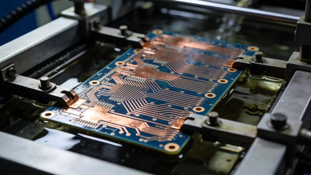
3. Copper Deposition (Chemical Copper Plating)
Following drilling, manufacturers deposit a thin layer of chemical copper inside the drilled holes and on the substrate surface. This chemical reaction coats non-conductive epoxy glass cloth (or other rigid substrates) with a conductive copper layer—enabling electrical continuity between layers and preparing the surface for subsequent electroplating.
4. Full-Board Copper Plating
Subsequently, manufacturers electroplate the entire board to thicken and protect the thin chemical copper layer. This step prevents oxidation of the copper in air, which would otherwise lead to broken connections or hole defects (e.g., copper voids). The goal is to create a uniform, durable copper base that supports reliable circuit formation.
5. Circuit (Pattern Transfer)
In this stage, manufacturers apply dry film or screen-printed anti-electroplating ink to the board. They expose the board to UV light through a photomask (with the desired circuit pattern) and develop it—removing unexposed ink/dry film to reveal the circuit layout. This step transfers the digital design to the physical substrate with high precision.
6. Pattern Electroplating
To meet current-carrying capacity requirements, manufacturers electroplate copper onto the exposed circuit patterns. They thicken the copper in holes and on circuit traces to a specified thickness, ensuring the rigid PCB can handle its intended electrical load without overheating or failure.
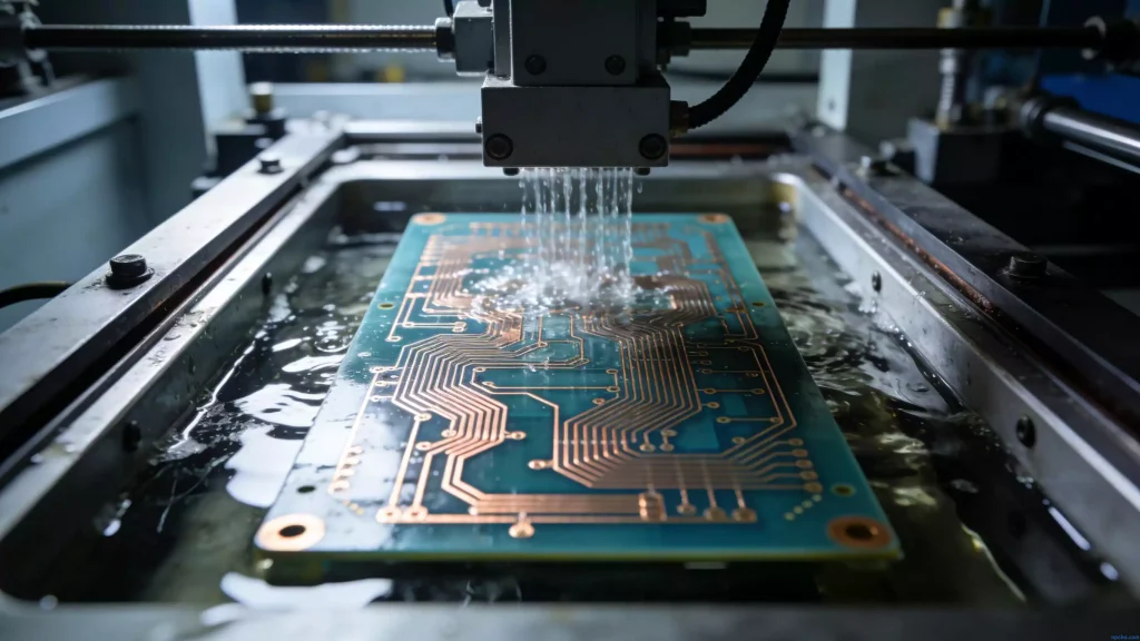
7. Etching
After pattern electroplating, manufacturers strip away the remaining anti-electroplating ink or dry film. They immerse the board in an etching solution, which removes excess copper foil (areas not protected by the ink/dry film), leaving only the desired conductive circuit patterns on the substrate.
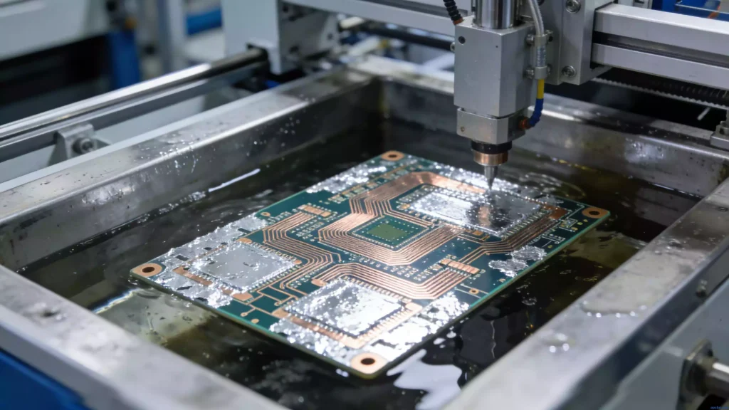
8. Tin Stripping
Next, manufacturers remove the tin layer (used as a protective mask during pattern electroplating) from the formed circuit patterns. This exposes the clean copper surface needed for soldering and prevents tin from interfering with component installation later.
9. Solder Mask Application
Additionally, manufacturers screen-print a layer of solder mask ink (or apply solder mask dry film) to the board. They expose and develop it to create a solder mask pattern, which protects circuit traces from short circuits during soldering, prevents copper oxidation, and boosts the rigid PCB’s long-term durability.
10. Gold Plating/Tin Spraying
For solder pad preparation, manufacturers deposit gold or tin on the board’s solder pads (areas where components will be soldered). Gold plating offers superior corrosion resistance and solderability, while tin spraying is a cost-effective alternative—both options prevent copper oxidation and ensure reliable component bonding. Learn more about specialized plating techniques in our guide: What Is PCB Side Plating? Types, Applications & Benefits.
11. Legend Printing (Character Printing)
Subsequently, manufacturers print iconic characters, part numbers, and component labels on the board. These legends help engineers and assemblers correctly install components, reducing errors during the final assembly process and simplifying maintenance.
12. Stamping/Forming
To meet mechanical design requirements, manufacturers cut or stamp the rigid PCB into the final shape specified by the customer. This step ensures the board fits perfectly into the target electronic device, aligning with the product’s form factor.
13. Electrical Testing
Finally, manufacturers test the finished rigid PCB electrically to detect open circuits, short circuits, or poor connectivity. Common methods include continuity testing and insulation resistance testing—ensuring the board meets all electrical performance standards before delivery to the customer.
opcba.com provides a one-stop rigid PCB manufacturing service, covering every step of the production process with 15+ years of industry experience. Whether you need custom rigid PCB design, production, or testing, contact our team today for personalized support.


