Anyone who’s worked in PCB fabrication knows a well-made board isn’t just about following design files—it’s about nailing the small details that impact manufacturability, performance, and yield.
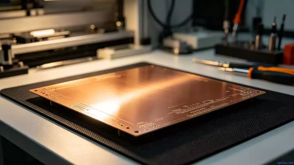
A printed circuit board (PCB), also called a printed wiring board (PWB), starts as a design and becomes a physical product through a series of precise steps.
The design specs you follow here make all the difference—none more so than “balanced copper.”
In real production, balanced copper isn’t just a recommendation; it’s a must.
Each layer in the PCB stack needs consistent copper coverage to avoid electrical glitches and mechanical issues that can derail circuit performance.
What Does PCB Balanced Copper Actually Do?
PCB balanced copper serves several key purposes in board manufacturing—most of which tie back to reliability and cost savings.
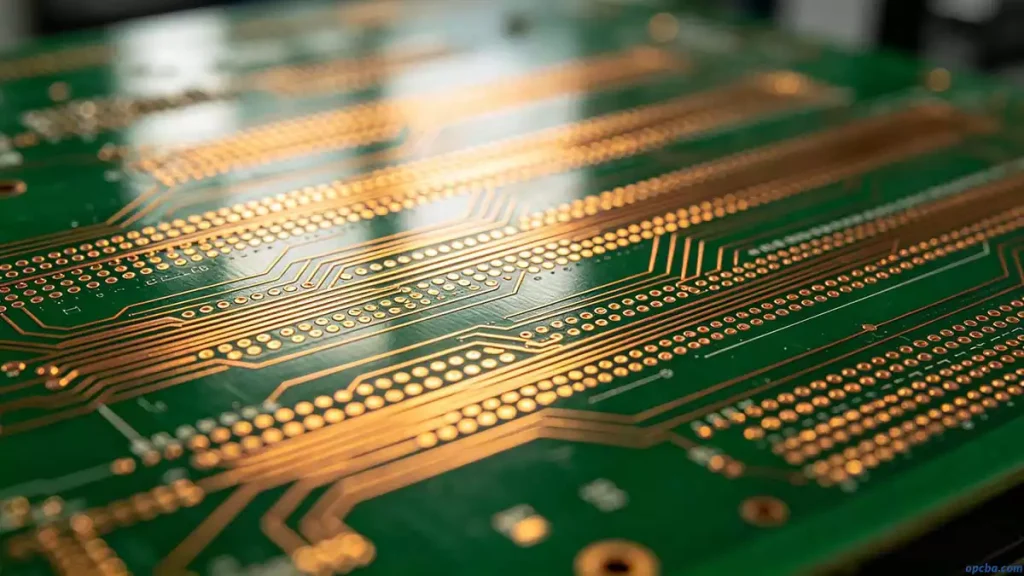
Copper layers get etched to form circuit traces, and those traces carry both signals and heat across the board.
Balanced coverage keeps the board from heating unevenly, which we’ve found cuts down on internal trace breakage over time.
It also acts as a built-in heatsink for power circuits.
Instead of adding extra heat-dissipating components, the copper itself does the work—saving both time and manufacturing costs.
Balanced copper also boosts conductor and pad thickness.
By plating copper onto the board (and through holes), we create stronger interlayer connections that hold up better during assembly and use.
Another big win: it reduces ground impedance and voltage drop.
This cuts down on electrical noise and improves power supply efficiency—critical for high-performance boards.
What Happens When Copper Isn’t Balanced?
We see this all the time in production: unbalanced copper distribution across stacked layers leads to avoidable problems.
Warping (what we call the “potato chip effect”) is common, as is poor plating on conductive patterns.
These issues don’t just hurt yield—they can render entire batches of boards unusable.
Practical PCB Balanced Copper Design Specs
Designing for balanced copper doesn’t have to be complicated, but it does require attention to detail.
Here are the guidelines we follow on the floor to keep boards consistent and reliable.
Start with Stack-Up Symmetry
During stack-up design, we usually recommend setting the center layer to the maximum copper thickness.
Then we balance the remaining layers to match their mirror counterparts—this helps avoid the warping we mentioned earlier.
Use Grids for Wide Copper Areas
Wide solid copper areas can throw off layer density.
Instead of solid planes, we design these areas as grids.
It’s a simple tweak that largely prevents bowing and twisting in the final board.
Symmetrical Power Layers
Power layers should be placed symmetrically in the stack, with the same copper weight on each.
This keeps the board balanced and ensures consistent power delivery across all layers.
Don’t Forget Core & Prepreg Layers
Balanced copper isn’t just for signal or power layers—it matters for core and prepreg layers too.
Maintaining an even copper ratio here keeps the entire board stable, from top to bottom.
Balance Excess Copper with Grids
If one layer has excess copper, we add tiny, unconnected copper grids to its mirror layer to balance it out.
These grids don’t connect to any network, so they won’t interfere with board functionality—just make sure they don’t impact signal integrity or impedance.
Wrapping It Up
Printed wiring board (PWB) performance and manufacturing yield hinge on small, intentional design choices—balanced copper chief among them.
By following these practical guidelines, you can avoid common pitfalls like warping and poor plating, while boosting overall board reliability.
In the end, balanced copper is one of those details that separates a good PCB from a great one—simple to implement, but critical to success in PCB fabrication.


