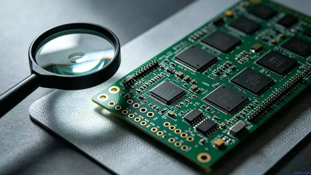
Through-holes connect different layers on a PCB and carry electrical signals between them. As electronics keep evolving, PCB fabrication and SMT assembly have to meet tighter quality and density requirements.
Modern products demand highly integrated circuits and compact internal layouts. PCBs have moved steadily toward higher density and finer structures, with SMT, BGA and HDI designs becoming standard in most advanced assemblies. This is why through-hole plugging has become a common requirement from manufacturers during assembly.
In actual production, PCB through-hole plugging serves five key functions that directly affect yield and long-term reliability:
- Keep solder from leaking through vias during wave soldering, which avoids short circuits on component surfaces. This is especially important for vias inside BGA pads—holes must be plugged before gold plating to support stable BGA soldering.
- Prevent flux from getting trapped inside vias, where it can degrade performance over time.
- Allow proper vacuum testing after components are mounted, since open vias would break the negative pressure environment.
- Stop surface solder paste from flowing into holes, which often leads to insufficient solder and poor mounting results.
- Reduce the risk of solder beads ejecting during wave soldering, a frequent cause of unexpected shorts on dense boards.
Common Types of PCB Through-Hole Plugging
Different plugging methods suit different board designs, hole sizes and end applications. Two approaches are most widely used in the industry.
Resin Through-Hole Plugging
This method uses solvent-free ink to fill vias. It avoids the uneven filling seen with traditional inks and lowers the chance of cracking when exposed to heat. It works especially well for vias with consistent vertical and horizontal dimensions.
resin through-hole plugging brings clear advantages for dense and high-end PCBs:
- It allows tighter hole spacing around BGAs and makes routing much easier in crowded layouts.
- For buried vias in HDI boards, it helps balance dielectric thickness and filling requirements.
- On thicker boards, it improves overall mechanical and electrical reliability.
- It supports VIP (via in pad) processes, where vias are drilled directly inside BGA pads. Without resin plugging, these vias often leak solder and create cold joints on the mounting side.
The PCB via plugging process for resin includes drilling, plating, hole filling, baking and grinding. After the via walls are plated, resin is applied and cured, then the surface is ground flat. Since the cured resin area has no copper, an extra plating step is needed to form usable pads. These steps happen early in production, before standard board-wide drilling and processing.
Air bubbles can form if plugging is done poorly. While bubbles alone don’t always ruin a board, they absorb moisture that can cause delamination or popping during reflow. Bubbles also push resin outward while baking, leaving uneven surfaces that are easy to catch in quality checks.
Electroplating Filler
This approach uses special additives to control copper growth, filling vias with pure copper. It is mostly used for stacked blind holes in multilayer boards or designs that carry high current.
Benefits of electroplated filling include:
- It simplifies layout for stacked vias and via-in-pad structures.
- It supports better signal behavior in high-frequency designs.
- Hole filling and electrical connection happen in a single step.
- Copper-filled blind holes offer better reliability and conductivity than conductive adhesive alternatives.
Hot Air Leveling and Plugging Process Sequences
Factories typically use two process orders for HAL and via plugging, each with its own pros and cons.
HAL before Plugging
Flow: Solder mask → HAL → hole plugging → curing. After hot air leveling, vias are plugged using aluminum or ink screens. Photosensitive or thermosetting ink can both be used.
This method prevents ink loss from vias after HAL, but it often leaves ink stains on the board surface and uneven filling, which can hurt later soldering.
Plugging before HAL
Several variations are commonly used:
- Plug holes with aluminum sheets → cure → grind → pattern transfer.
- Plug holes with aluminum sheets → directly apply solder mask.
- Plug holes with aluminum sheets → develop → pre-cure → grind → solder mask.
- Apply solder mask and plug holes at the same time.
The best sequence mostly depends on design density and assembly needs. For high-density boards, we usually suggest plugging before HAL to avoid surface contamination.
If you need support with PCB through-hole plugging for your project, opcba can help. Our team has hands-on experience optimizing plugging processes for all kinds of PCB structures, ensuring consistent quality and high production yield.


