PCB chip and semiconductor packaging terminology is essential for electronics engineers, PCB designers, and manufacturing professionals to understand advanced IC assembly and packaging technologies. Specifically, this comprehensive guide breaks down the most common PCB chip terminology, providing accurate definitions, core features, and real-world application scenarios for each term.
COB (Chip On Board)
COB, short for Chip On Board, is a PCB assembly technology where manufacturers bond bare IC dies directly onto a printed circuit board via wire bonding, then encapsulate the dies with epoxy resin for protection. Notably, it offers high integration, low cost, and reliable electrical performance, and finds wide use in consumer electronics, LED lighting, industrial controls, and automotive electronics.
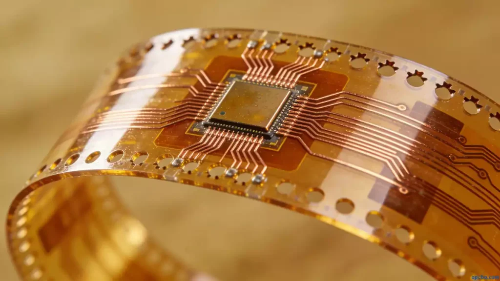
COF (Chip On Flex)
COF, short for Chip On Flex, refers to a packaging technology that mounts and bonds semiconductor chips directly onto flexible printed circuits (FPCs). In addition, it enables thin, lightweight, high-density designs, and serves commonly in display driver ICs, camera modules, wearable devices, and flexible electronics.
COG (Chip On Glass)
COG, short for Chip On Glass, bonds IC dies directly onto glass substrates such as LCD or OLED display panels. Furthermore, it minimizes module size and signal interference, and finds common application in mobile screens, smart watches, automotive dashboards, and industrial displays.
FTN (Formulated STN)
FTN, short for Formulated Super Twisted Nematic, is an enhanced STN LCD technology that adds an optical retardation compensation film to boost contrast and widen viewing angles. Specifically, it primarily serves monochrome black-and-white displays in low-power instruments and consumer electronics.
TCP (Tape Carrier Package)
TCP, short for Tape Carrier Package, is a flexible circuit packaging solution that mounts IC dies on polyimide tapes with prefabricated copper circuits. Additionally, it enables high I/O density and automated assembly, and often appears in display driver ICs and portable electronic devices.
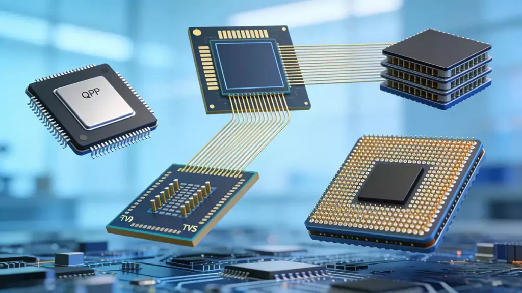
QFP (Quad Flat Package)
QFP, short for Quad Flat Package, is a surface-mount IC package with gull-wing leads extending from all four sides. Moreover, it delivers a high pin count, excellent solderability, and strong thermal performance, and finds wide use in MCUs, automotive ICs, and industrial control chips.
QTP (Quad Tape Carrier Package)
QTP, short for Quad Tape Carrier Package, is a four-sided tape carrier package that merges the flexibility of TCP with the high-pin layout of QFP. As a result, it serves high-I/O chips in automotive and industrial electronics.
SMT (Surface Mount Technology)
SMT, short for Surface Mount Technology, stands as the most prevalent PCB assembly method, where manufacturers mount components directly onto the board surface without drilling through-holes. Consequently, it enables miniaturization, high density, and automated mass production for modern electronics.
TSV (Through Silicon Vias)
TSV, short for Through Silicon Vias, serves as a core interconnection technology for 2.5D and 3D packaging. Specifically, it employs copper-filled vertical channels that run through silicon dies or wafers to create the shortest possible electrical path between chip surfaces. In turn, TSVs cut signal delay, boost bandwidth, and enable high-density vertical integration.
2.5D Packaging
2.5D packaging represents an advanced IC packaging evolution from traditional 2D planar designs. In this setup, engineers place multiple dies side-by-side on a silicon interposer layer embedded with TSVs. Furthermore, the interposer delivers stable, high-density interconnections between chips, making it widely used in high-end ASICs, FPGAs, GPUs, and High Bandwidth Memory (HBM) systems.
3D Packaging
3D packaging takes integration a step further by vertically stacking multiple logic dies, memory dies, or heterogeneous chips, using TSVs or micro-bumps for direct vertical interconnection. Unlike 2.5D packaging, it drastically shrinks the package footprint, shortens signal paths, and boosts power efficiency. As a result, it finds wide application in 3D DRAM, HBM, AI chips, and high-performance computing systems.
RDL (Redistribution Layer)
RDL, short for Redistribution Layer, is a metal wiring layer with copper traces and polymer dielectrics that reroutes chip I/O pads to a more flexible, practical layout. Additionally, it enables seamless interconnection between dies and packages, forming a core structure in 2.5D, 3D, and FOWLP advanced packaging solutions.
FOWLP (Fan-Out Wafer-Level Packaging)
FOWLP, short for Fan-Out Wafer-Level Packaging, is an advanced wafer-level packaging innovation. Typically, it embeds diced dies in epoxy molding compound to form a reconfigured wafer, then fabricates high-density RDL and solder balls on its surface. Compared to traditional WLP, it delivers more I/O, a smaller footprint, and superior electrical performance.
Fan-Out Packaging
Fan-out packaging “fans out” I/O connections beyond the chip area using molding compound and RDL, achieving more external pins in a compact form factor. Moreover, it eliminates the need for interposers and streamlines heterogeneous integration of multiple dies. Consequently, it offers high I/O density, a small footprint, and low cost for mobile and IoT devices.
Interposer (Intermediary Layer)
An interposer (or intermediary layer) acts as an intermediate substrate in multi-die advanced packaging, bridging chips and the main PCB. It can use silicon, organic, or glass materials as its base. Notably, silicon interposers support high-density I/O and TSV integration, playing a critical role in 2.5D and 3D packaging solutions.
By mastering these PCB chip and semiconductor packaging terms, you can confidently select the optimal assembly and packaging solution for your project. Furthermore, for custom PCB manufacturing, advanced IC packaging support, or professional electronics manufacturing services, reach out to opcba.com.


