Filter posts by category
Communication Device
Imagine a slim smartphone handling crystal-clear calls worldwide. Or a remote IoT sensor sending data perfectly in tough conditions. The circuit board
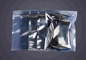
A Comprehensive Guide to PCBA Packaging
As the electronics market continues to expand, PCBA (printed circuit board assembly) packaging methods are becoming increasingly important. To ensure that products are delivered
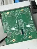
PCB with Better Heat Dissipation: Aluminum Substrate
1. What is an aluminum substrate PCB? PCB also known as a printed circuit board. Aluminum substrate is a type of PCB. Aluminum substrate is
Innovative Applications of PCB Overmolding Technology
In today’s rapidly evolving electronics industry, flexible printed circuits (FPCs) have become indispensable components in products ranging from medical wearables to automotive
Rogers Laminate – The Optimal Solution for High-End Applications(2)
PCB (Printed Circuit Board) is an essential component of modern electronic products. It forms a multi-layered structure by stacking circuit boards, enabling more
Rogers PCB Laminate – The Optimal Solution for High-End Applications(1)
This article is mainly a summary of Rogers RF PCB materials. Rogers’ RO4000® series of hydrocarbon ceramic laminates and prepregs have consistently led the
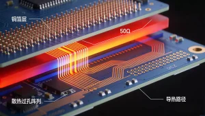
PCB: The AI Evolution of the “Mother of the Electronics Industry” (Ⅱ)
AI servers continue to pursue greater speed, performance, and capacity. PCBs are seeing corresponding upgrades to their parameters and performance. High-end servers
PCB: The AI Evolution of the “Mother of the Electronics Industry” (Ⅰ)
The electronics industry is experiencing robust growth driven by the explosive demand for AI computing power, with PCB emerging as a particularly prominent player as
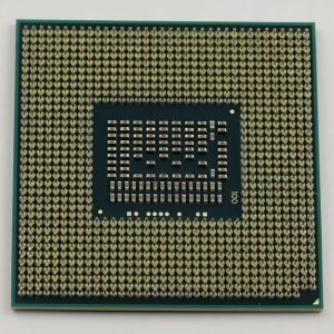
What Is an IC Substrate? — A Comprehensive Guide to Functions, Types, Technical Specifications, and Industry Challenges
An IC substrate is a PCB used to package microchips. It can also be referred to as an IC carrier board. It connects the

FPC Raw Materials: What You Need to Know
FPCs are highly reliable, exceptionally flexible printed circuit boards manufactured using polyimide or polyester film as the substrate material. They feature high
AI-Driven PCB: The Cornerstone of Next-Gen Computing Power
AI servers evolve for faster speed, higher performance and larger capacity, so PCB parameters and performance improve accordingly. The prior article introduced
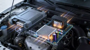
Automotive Electronics
Automotive Electronics rely on robust switching power supplies to deliver stable performance in extreme vehicle environments—from engine bay heat to road vibrations.
Aerospace
Aerospace is an industry defined by uncompromising safety, extreme environmental demands, and rigorous compliance. Even the smallest component failure can have catastrophic
Power and Energy
Power and energy are the lifelines of modern electronic systems. For high-reliability applications like aerospace avionics, industrial automation, and satellite communications, even
Millimeter wave radar
Millimeter wave radar is a cornerstone of modern sensing technology. It enables precise detection, ranging, and speed measurement across diverse high-demand industries.
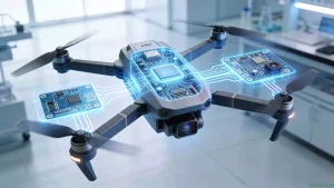
Consumer Drone
Consumer drone is a mainstream recreational unmanned aerial vehicle (UAV). Its core performance — including flight stability, miniaturization and functional integration —