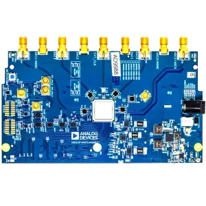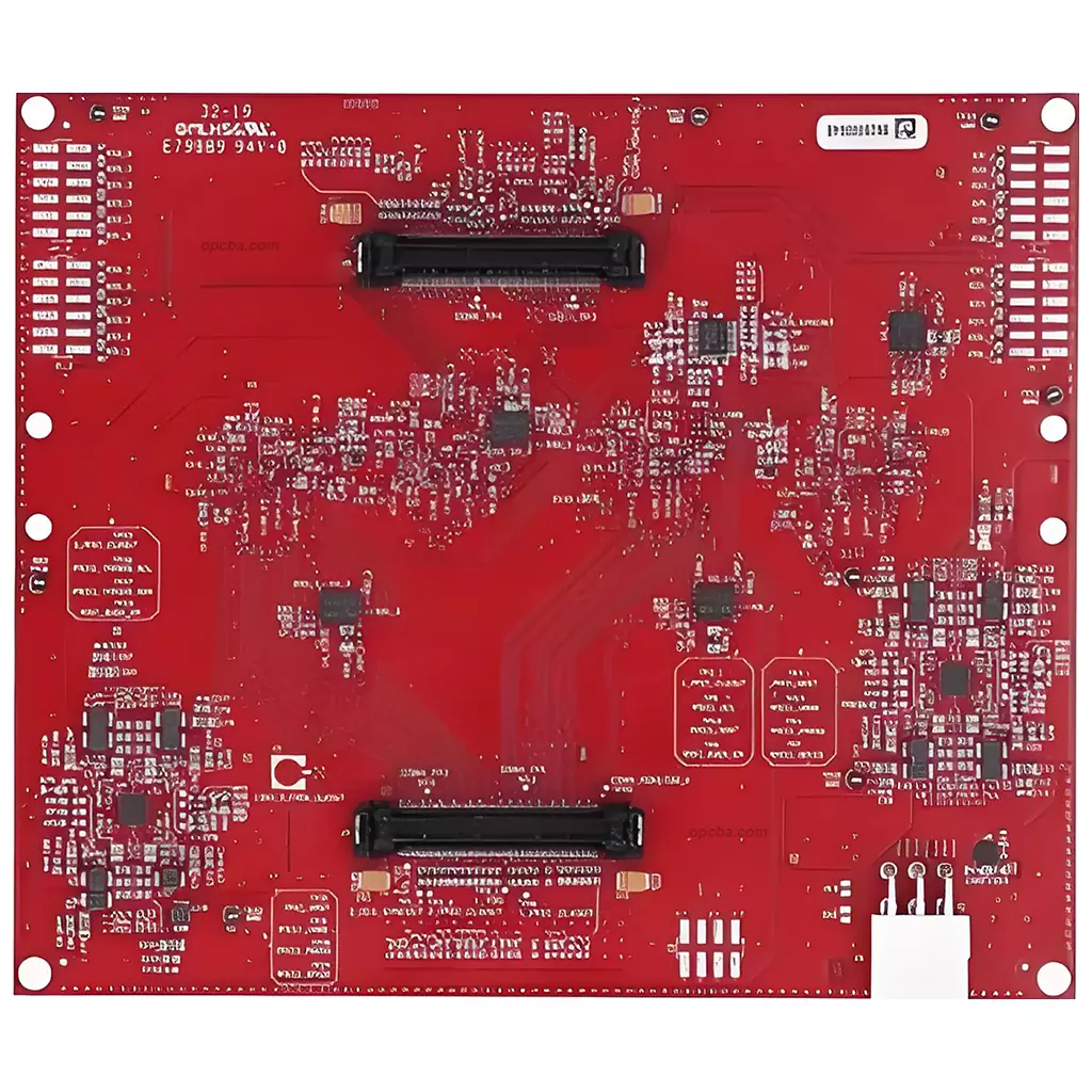
Overview of PCBA
PCBA stands for Printed Circuit Board Assembly. It is the unit that exists once components have been soldered, assembled and tested onto a bare PCB. The bare board supplies the copper pattern and the interconnect between parts; the assembly turns that pattern into a working circuit. Across most electronic equipment, it is the assembly that decides whether the product meets its specification and holds up in service.
Assembly work starts before the first component is placed and continues after the last joint is inspected. Incoming material checks, component verification, paste deposition, placement accuracy, thermal profiling, cleaning and electrical test all belong to it. The tolerance a shop can hold at each of those steps sets the ceiling on what a design can ask for, and the range our lines hold is published on our capability sheet.
PCBA Core Definition and Positioning
PCBA is the stage where a board stops being a pattern on laminate and becomes a tested electrical unit.
- Printed Circuit Board Assembly covers the board, the components and the joints between them, delivered as one tested unit.
- A PCB carries no components and cannot perform a function by itself. Populating and soldering it is what makes the board directly usable inside equipment.
- The assembly stage settles electrical function, mechanical retention and the thermal path at the same time. Holding all three in one process removes a step from the customer’s line and shortens the path from a design to a working sample.
Core Components of PCBA
- The bare board supplies the mounting surface and the interconnect. It is built as single-sided, double-sided, multilayer or HDI construction, depending on density and layer count.
- Active devices such as ICs and chips carry the switching and the processing. Passive devices such as resistors and capacitors set operating points and hold the supply steady.
- Connectors and switches carry signals and power on and off the board. Fuses and similar protective parts interrupt the path when something goes wrong, and mounting hardware locates the assembly inside the enclosure.
- Solder paste, flux, thermal interface materials and adhesives join the parts and manage heat. Their selection follows the board finish and the thermal profile the build will see.
Core Production Process of PCBA (8-stage Simplification)
The sequence below is the standard path our assembly lines run. Steps that a given design does not need, such as through-hole insertion, are skipped.
- PCB incoming inspection (IQC): checking circuits, hole diameters and surface condition before a board enters the line.
- Component incoming inspection and material preparation: verifying model parameters and sorting materials, so that wrong or damaged parts never reach placement.
- Solder paste printing: depositing paste on the pads at controlled thickness and accuracy, since paste volume is the largest single influence on joint quality.
- SMT assembly: placing components onto the pads and holding placement accuracy across the panel.
- Reflow soldering: melting the paste under a controlled thermal profile, so the joints form without damaging the board or the parts.
- DIP insertion welding, where the design calls for it: through-hole parts are inserted and soldered, by hand or automatically, to a firm joint free of short circuits.
- Cleaning and repair: removing flux residue and other contaminants, then reworking any shorts or loose joints found.
- Final inspection (FQC) and packing: checking appearance and function, then packing against static and moisture damage for shipment.
Most boards carry a mix of package types, so the order of the two soldering steps matters. Surface-mount parts go on first and reflow together; through-hole parts are inserted afterwards and soldered on their own pass, which keeps the finished surface-mount joints from being reheated. The routing and stencil decisions behind both paths are covered in our SMT and through-hole assembly guide.
Cleaning and final inspection are backed by checks that run through the whole sequence. Every stage releases a panel only after it clears an inspection gate, and the acceptance rules applied at those gates are set out on our quality control page.
PCBA Multi-Field Applications
Assembly work reaches nearly every product category that carries electronics, and the requirements shift with the environment the unit will see.
- Consumer electronics, smart home devices and internet of things products favour compact outlines and dense placement at a low unit cost. Our smart home control boards are one example.
- Automotive electronics face vibration, thermal cycling and long service life, which push toward heavier copper, high Tg laminate and tighter process control.
- Industrial control and medical technology run long product lives, so traceability and repeatability matter as much as first-pass yield.
- Communication equipment carries high speed links in continuous operation, which puts impedance control and thermal design at the centre of the build.
- Military and aerospace work follows published acceptance standards, with residue control and documentation held to tighter limits.
Board size, component count, package mix and test depth all move the process, which is why two assemblies with the same board area can need very different lines.