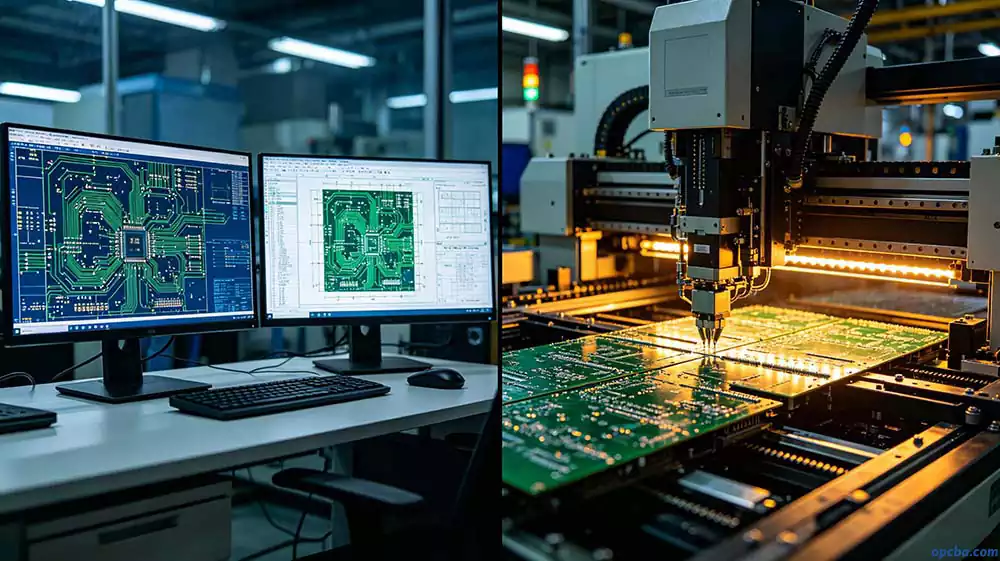
Every PCB design goes through the same transition: from layout screen to factory floor. What happens in that handoff determines whether your board ships on time or gets stuck in a loop of revisions, re-spins, and rising costs.
Design for Manufacturing is the engineering discipline that manages this transition. It’s a systematic review of your Gerber files, BOM, and assembly data against the physical realities of fabrication and assembly — trace widths that can actually be etched, solder mask bridges that will actually prevent shorts, pad geometries that will actually form reliable joints. Done right, PCB DFM catches the issues that simulation software misses, because simulation doesn’t know what a worn stencil or a high-humidity production day does to yield.
At OPCBA, every order goes through this review — prototypes and volume production alike. It’s not a premium add-on. It’s how we ensure the boards we ship match the boards you designed.
What Skipping DFM Costs You
The costs of skipping PCB DFM are easy to calculate and hard to recover.
Money. One design revision means redoing the entire engineering setup. If stencils and fixtures are already cut, you’ll pay for another set. Two or three re-spins, and a project burns through its hardware budget before reaching market.
Time. Every revision cycle — fab feedback, engineering evaluation, layout changes, re-submission — adds a week or more. A 10-day lead time stretches to 25 days. For products with a hard launch date, that window doesn’t reopen.
Yield. Without DFM optimization, first-pass SMT yield can settle at 85%. That means 15 out of every 100 boards need rework — jumper wires, touch-up soldering, component swaps — all manual, all unpredictable, all eating into margin.
I once traced a field failure pattern back to a single missing thermal via array under a BGA. The boards passed functional test at the factory, but solder joint voiding above 25% turned every board into a latent failure. The fix was simple — add the vias — but the lesson was expensive: what passes test isn’t necessarily reliable.
What We Review
We generate a DFM report for every order. The review covers two domains: can the bare board be built, and can the assembly run smoothly.
PCB Fabrication
Trace width and spacing. Below 3 mils, etched traces develop a trapezoidal cross-section — narrower at the top, wider at the bottom — making controlled impedance difficult to hold.We flag every location that doesn’t meet minimum width and spacing, with suggested adjustments. To learn more about making these critical design choices early in your layout process, check out our guide: How to Choose Trace Width and Spacing for Your PCB Design
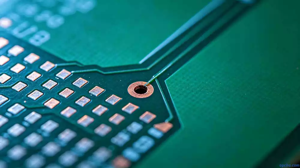
Vias and annular rings. An undersized annular ring combined with normal drill wander produces an open circuit. We require 5 mils minimum for mechanical vias and 3 mils for laser vias. Anything below that is documented with coordinates and recommended corrections.
Solder mask bridge. Between 0.5mm-pitch QFP pads, a solder mask bridge thinner than 4 mils is a bridging risk. We recommend reducing pad openings or switching solder mask color — green offers the tightest registration tolerance.
Material and stackup. We verify that your specified laminate and prepreg combination can achieve the target thickness, that the dielectric constant aligns with your impedance calculations, and that the copper weight supports the current requirements. For hybrid boards — Rogers on RF layers, FR-4 on digital layers — we cross-check the CTE mismatch to ensure lamination won’t cause separation.
Board edge and panelization. We check copper-to-edge clearance, V-cut depth versus trace proximity, and whether the breakaway rails provide enough width for SMT equipment clamping. Fiducial count and placement are verified against pick-and-place requirements.
PCBA Assembly
Pad design. For BGAs and QFNs, we confirm whether pads use SMD or NSMD definition against the component datasheet. NSMD pads offer better solder wetting; SMD pads offer tighter placement tolerance. The choice matters for yield.
Component spacing. We check that tall components won’t collide with pick-and-place nozzles reaching adjacent short parts, and that the clearance between wave-soldered through-hole components and SMD devices accommodates pallet fixture shielding.
Test points. We verify that ICT and FCT test points are present and probe-accessible. A BGA without test points forces X-ray inspection as the only verification method, doubling inspection cost. We recommend adding test access early.
Panelization and depaneling. We check whether V-cut paths pass near ceramic capacitors that could crack during depaneling, whether tab-routing spacing supports the board weight, and whether sensitive components sit near the break line.
What a DFM Report Looks Like
Our DFM report documents every finding with four data points: exact coordinates, a marked screenshot, the design rule violated, and a specific correction recommendation.
For example: “Pad spacing under U12 measures below 4 mils — bridging risk. Recommend reducing pad opening by 0.5 mil per side, or adjusting trace routing to increase separation.” No guesswork. No back-and-forth.
How DFM Saves You Money
Design for Manufacturing is fundamentally a cost-prevention practice.
Material utilization. Optimized panelization can yield 15%–20% more finished boards from the same raw panel, directly lowering unit material cost.
SMT first-pass yield. DFM-reviewed designs consistently reach 98% or higher first-pass yield, eliminating most of the manual rework that drives assembly cost.
Predictable lead times. When the design is right the first time, production doesn’t stall. There are no emergency revision calls, no expedited re-spins, no sunk engineering hours on fixing what should have been caught earlier.

Start Your DFM Review
We don’t reserve DFM reviews for large orders. Every prototype gets the same DFM report as volume production.
Send your Gerber files, BOM list, and pick-and-place file to sales@opcba.com. Include any special requirements — impedance control targets, specific laminates, surface finish preferences. We’ll complete the engineering review, return a formal quote with DFM feedback, and call immediately if any critical issues need discussion.
Design for Manufacturing isn’t a gate to pass. It’s the standard practice that separates predictable production from constant firefighting. We apply it to every board we build.


