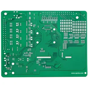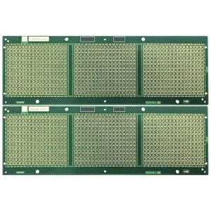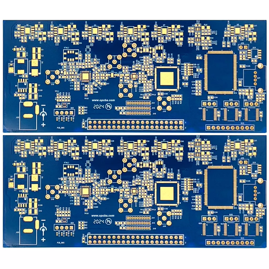
2-layer-PCB(Double-layer Printed Circuit Board)Product Description
1.Product Definition
First, a 2-layer-PCB (Double-layer Printed Circuit Board) is a basic, widely used PCB type.
Its core structure has two conductive copper foil layers.
An insulating substrate (commonly FR-4) separates these two layers.
Vias establish electrical connections between the two circuit layers.
Additionally, it boasts compact structure, controllable cost and stable performance.
Thus, it becomes one of the most commonly used PCBs in electronic devices.
2.Core Features
2.1 Simple Structure & Controllable Cost
Compared to multi-layer PCBs, it has a simpler structure and process.
It also has a shorter production cycle and high cost-effectiveness.
Therefore, it suits batch production needs well.
It is the preferred choice for small and medium power electronic devices.
2.2 Double-Sided Wiring & High Space Utilization
Both upper and lower layers can have conductive lines.
This effectively saves board space.
It can achieve more circuit functions in a limited size.
As a result, it meets miniaturized equipment design requirements.
2.3 Stable Electrical Performance
It uses high-quality insulating substrates like FR-4.
Its copper foil has uniform thickness and reliable via connections.
It also has good insulation, heat resistance and anti-interference ability.
These features ensure its stable operation.
2.4 Wide Adaptability & Convenient Processing
It supports conventional surface treatments (gold plating, tin spraying, OSP, etc.).
It can match SMT assembly, insertion and other methods.
Moreover, it meets different electronic component installation needs.
2.5 High Customization
We can customize its copper foil thickness (0.5oz – 3oz).
We also customize substrate material, line width and spacing.
In addition, via specifications are customizable.
This flexibility adapts to different scenario electrical requirements.