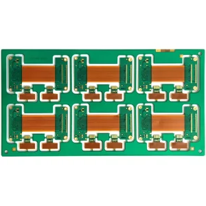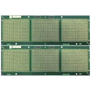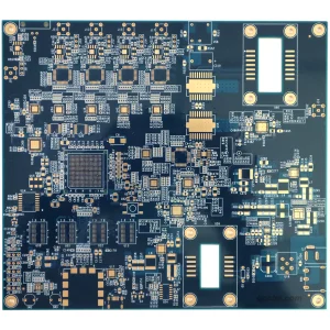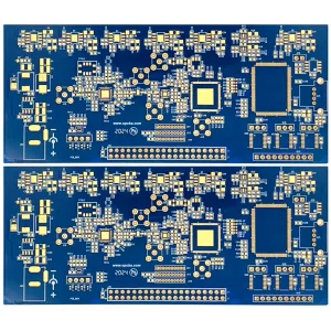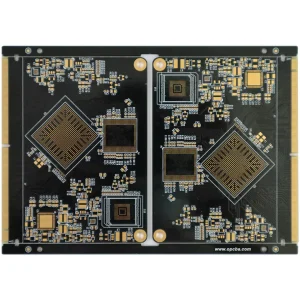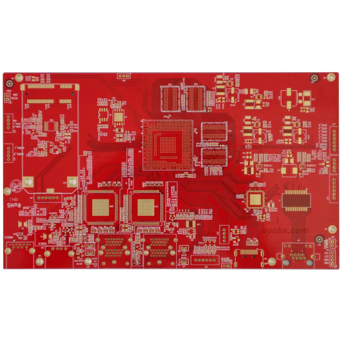
Overview of 6-Layer PCB
A 6-layer PCB sits between the four-layer stack and the eight-layer boards that need an extra lamination cycle. The two inner layers give a designer room to pull power and ground out of the signal layers, something a four-layer board usually cannot afford. Boards with moderate routing density and two or three supply rails tend to land here first.
Structural Composition
The common stack pairs signal layers on the outside with a ground plane and a power plane on the inside: signal, ground, power, signal. Copper thickness runs about 35 μm (1 oz) on the outer layers and 18 μm (0.5 oz) on the inner ones. Cores and prepreg sheets are laminated in a single press cycle, which holds layer-to-layer registration tighter than a higher layer count allows. Our PCB manufacturing process overview covers how that cycle works.
Key Design Considerations
Stack symmetry matters more than it looks. An unbalanced build warps during reflow, and six layers leave enough room to mirror the construction about the center. Three other points decide whether the design holds up.
- Signal integrity depends on keeping a reference plane adjacent to every high-speed trace, which is what the inner ground layer provides.
- Power integrity wants the plane pair close together, so the dielectric between ground and power should be as thin as the process allows.
- Impedance control sets the trace geometry. Targets of 50 Ω single-ended and 90 to 100 Ω differential are common, and the stack-up has to be fixed before routing starts.
Multi-Field Applications
Six layers cover a wide band of products:
- Consumer electronics: smartphones, tablets, laptops, and wearables.
- Industrial control: PLCs, sensors, and drive systems.
- Automotive: driver assistance modules, infotainment, and powertrain controllers.
- Telecom and networking: routers, base stations, and high-speed data equipment.
- Medical and aerospace: precision instruments and avionics.
Material Selection & Cost Reference
Standard FR-4 handles most six-layer work. Designs running above a few gigahertz need a low-loss laminate, and the price step for that material usually outweighs the cost of the extra layers.
Outer copper runs 35 μm and inner copper 18 μm in the standard build. Thicker copper carries more current, and etching it to fine geometry gets harder, so the heavier build brings its own cost.
On price, four layers to six is the first real step in the curve: roughly 1.5 to 1.8 times a comparable four-layer board at the same size and volume. An additional lamination and imaging cycle drives most of that increase; the laminate price moves less. In small runs, engineering and tooling add a further share that fades at volume.
The 1.5 to 1.8 times range comes from published 2026 China-manufacturer data for standard FR-4 boards.