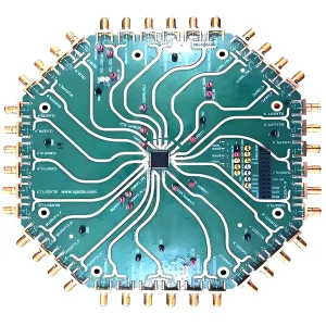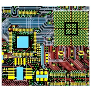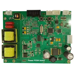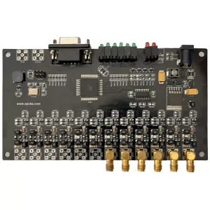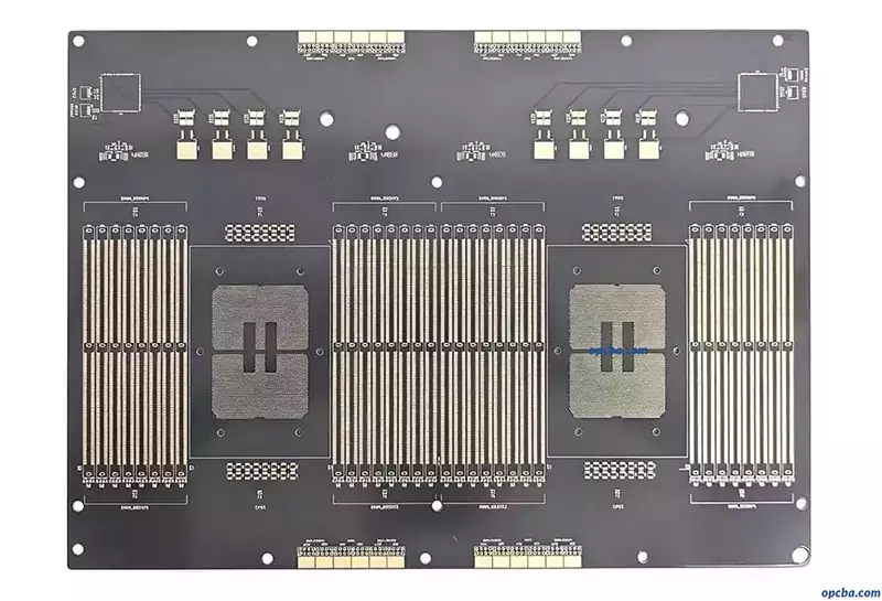
AI Server Circuit Board: Built for Stable Performance Under High Compute Load
Anyone designing hardware for modern AI compute racks knows the bottleneck isn’t always the GPU itself—it’s the board carrying the high-speed signals between chips, memory, and networking interfaces. A purpose-built AI Server Circuit Board has to maintain consistent signal integrity under 24/7 high compute loads while supporting demanding thermal, mechanical, and manufacturing requirements. If you’re new to core printed circuit board fundamentals and basic terminology, start with our foundational overview: Printed Circuit Board(PCB).
As AI hardware evolves toward faster interconnects, higher power density, and larger GPU clusters, PCB design becomes a critical factor in overall system stability. Material selection, stackup planning, impedance control, and fabrication quality all contribute to long-term performance.
Substrate Choice: The Foundation of Signal Integrity Under Load
The high-speed AI server PCB uses halogen-free substrates including Shengyi and TU-872 SLK low-loss, high-Tg laminates. All materials comply with halogen-free and RoHS environmental standards, but the real advantage becomes clear during continuous high-load operation.
In practice, standard mid-grade FR-4 may pass laboratory testing under light workloads. Once systems begin running at 80% or higher utilization around the clock, dielectric variation and increased insertion loss can gradually reduce high-speed signal margins. We’ve seen prototype projects pass initial validation only to encounter unexpected signal integrity issues during thermal chamber testing because the laminate simply wasn’t designed for sustained high-speed operation.
Choosing a low-loss, high-Tg material from the beginning reduces that risk and provides a more stable foundation for high-speed interfaces such as PCIe, Ethernet, and other high-bandwidth interconnects commonly found in AI computing platforms.
Manufacturing Capabilities for AI Server PCB Projects
Our standard manufacturing capability covers 4 to 24 layers, finished board thicknesses from 0.6 mm to 10.0 mm, and copper weights from 1 oz to 6 oz. This range supports everything from compact edge AI computing modules to large GPU carrier boards used in high-density AI training clusters.
Thicker copper isn’t only beneficial for carrying higher current—it also improves heat distribution across dense power delivery networks. However, heavy copper introduces its own manufacturing challenges. It requires tighter etching control, optimized lamination processes, and careful stackup planning to minimize board warpage and maintain registration accuracy.
There’s no universal “best” copper weight. The right choice depends on your power requirements, thermal targets, and overall PCB architecture.
Manufacturing Challenges Behind High-Speed AI Server PCBs
Designing an AI server PCB is only half the job—building it consistently is where manufacturing experience becomes critical.
High-layer-count stackups using low-loss materials demand precise lamination control, accurate layer registration, and stable resin flow throughout the press cycle. Heavy copper power planes, large BGA packages, and tightly controlled impedance traces all increase fabrication complexity.
During engineering review, our team evaluates stackup balance, impedance requirements, copper distribution, and manufacturability before production begins. For a full systematic breakdown of PCB stackup design principles, rules, and performance optimization methods, refer to our comprehensive guide: A Complete Guide to PCB Stackup: Structure, Types, Design Rules & Performance Optimisation. Early DFM review often identifies potential risks that can affect yield, reliability, or long-term performance, helping avoid costly revisions later in the project.
Surface Finish and Solder Mask Options for Reliable Assembly
We offer solder mask options in green, black, blue, and matte black, together with surface finishes including ENIG, immersion gold, and OSP. Minimum trace and spacing is 3 mil, supporting the fine-pitch routing required for today’s high-speed differential pairs and SerDes channels.
Matte black solder mask has become increasingly popular in AI hardware where internal optical components or imaging systems may benefit from reduced light reflection. Green, however, remains the preferred choice for most volume production because of its mature manufacturing process and excellent inspection visibility.
For most high-speed AI server PCB projects, especially those using 112G-class SerDes or similar high-speed interfaces, ENIG remains the preferred finish thanks to its excellent pad planarity, reliable solderability, and consistent assembly performance.
Applications Across Modern AI Computing Platforms
These boards are widely deployed across high-performance computing applications, including AI server platforms, GPU carrier boards, AI accelerator modules, cloud computing infrastructure, networking switches, high-speed communication equipment, edge AI systems, and HPC clusters.
Many repeat orders involve GPU carrier board designs where maintaining signal integrity across PCIe or other high-speed differential links has a direct impact on overall system performance. As signaling speeds continue increasing, maintaining consistent impedance, minimizing insertion loss, and ensuring manufacturing consistency become increasingly important throughout the entire PCB.
Whether the application is a large-scale AI training cluster or a compact edge inference device, reliable PCB manufacturing remains one of the key foundations for stable long-term operation.
Why Engineering Review Matters Before Production
Every AI server project has its own electrical, thermal, and mechanical requirements. Layer count, material selection, copper thickness, surface finish, and stackup design all need to work together.
Rather than applying a standard stackup, we review each project individually to recommend suitable materials and manufacturing processes based on your design goals. Early engineering review helps optimize manufacturability while reducing production risks and unnecessary redesign cycles.
Request a Custom Quote
Every AI Server Circuit Board is built to customer specifications—there is no one-size-fits-all solution.
Whether you’re developing a GPU carrier board, AI accelerator module, compute platform, or another high-speed computing system, our engineering team can review your Gerber files, recommend suitable laminate options, optimize the PCB stackup, and provide DFM feedback before production begins.
If your design is ready, simply send your Gerber files, stackup requirements, and estimated production volume to sales@opcba.com. We’ll prepare a formal quotation together with engineering recommendations to help move your project into manufacturing as efficiently as possible.
Frequently Asked Questions
What materials are recommended for AI server PCBs?
Low-loss, high-Tg laminates such as TU-872 SLK and selected Shengyi materials are commonly used because they provide better signal integrity and thermal stability than standard FR-4 during continuous high-speed operation.
Why is ENIG commonly used for AI server circuit boards?
ENIG provides a flat, reliable surface for fine-pitch BGAs and high-density components while offering excellent solderability and consistent assembly quality, making it a preferred finish for many AI server designs.
How many PCB layers does an AI server typically require?
Layer count depends on system complexity. Smaller edge AI devices may use fewer layers, while GPU carrier boards and high-performance computing platforms often require significantly higher layer counts to accommodate dense routing and controlled impedance requirements.
Can heavy copper improve AI server PCB performance?
Yes. Heavy copper can improve current carrying capability and heat distribution, but it also increases manufacturing complexity. Proper stackup design and fabrication control are essential to maintain board flatness and manufacturing yield.