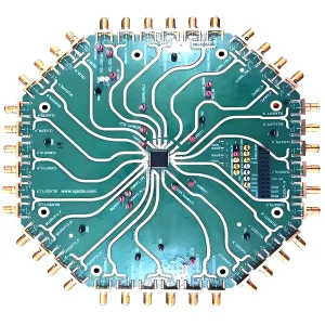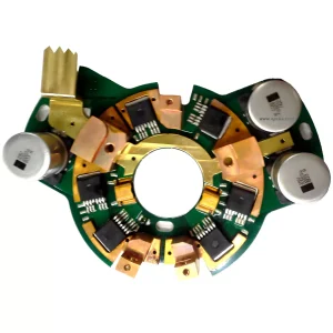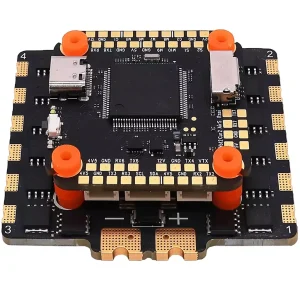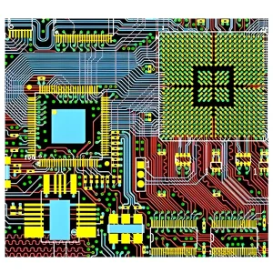
Overview of TV mainboard assembly
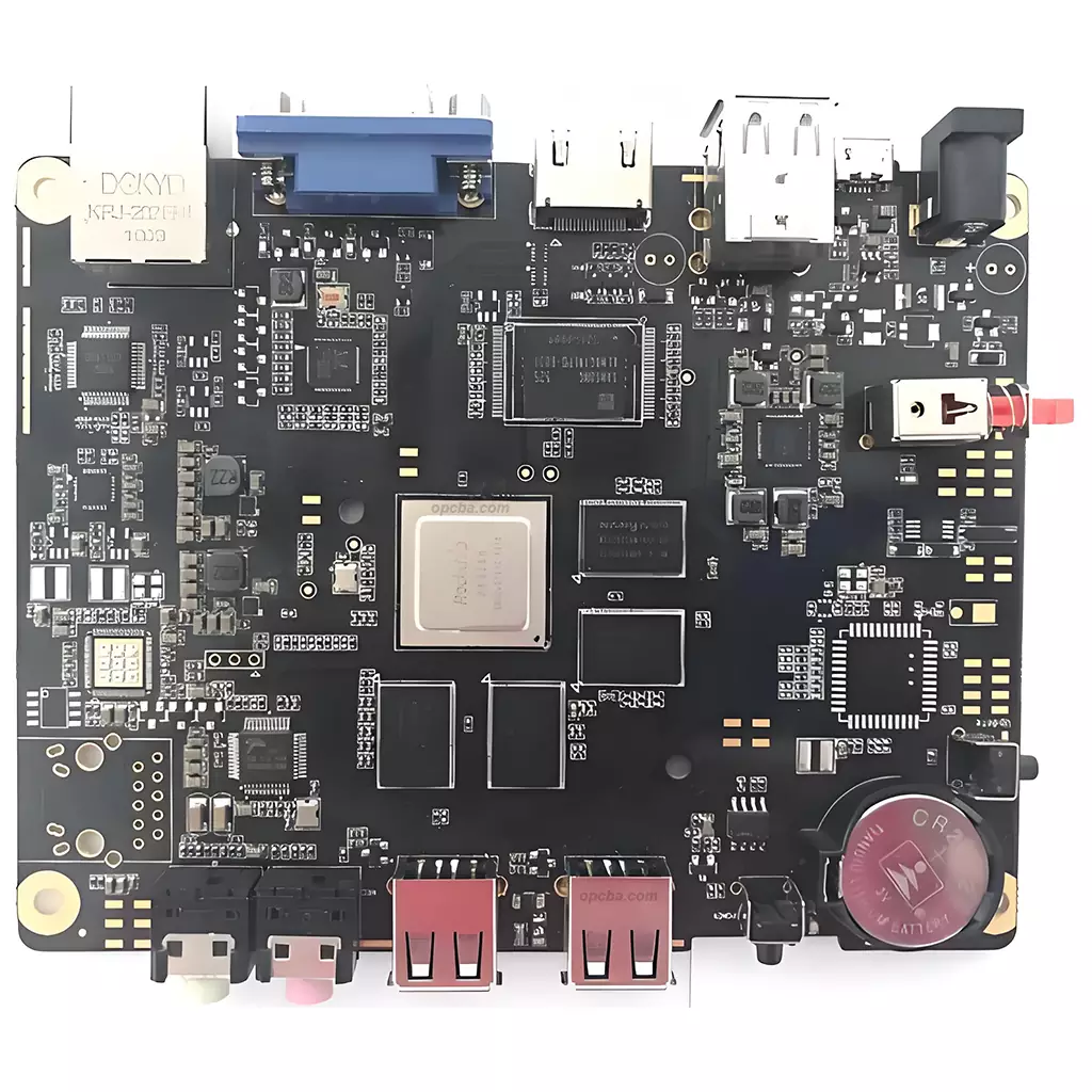
The board delivered here is fully populated and electrically tested. The finished board carries the processor, memory, power management and interface sections that drive the panel, and how those parts are placed and joined is what decides picture stability and service life. Mainboards in this class are large, densely populated, and built to fit a slim chassis.
What TV mainboards demand from a build
1. Board size: the mainboard is a large panel, so laminate lay up and bow and twist control carry more weight than they do on a small board.
2. Layer count: a basic HD set is often served by 4 to 6 layers, while Full HD and 4K designs commonly use 8 to 12 layers with HDI, and blind or buried vias to save space in a thin chassis.
3. High speed video interfaces: HDMI, LVDS and DDR links are impedance controlled, with HDMI and LVDS typically routed as 100 ohm differential pairs and length matched across the group.
4. Mixed signal and RF zones: video processing, digital logic and wireless modules share one board, so the analog and digital sections are separated and the wireless area is shielded.
5. Heat and power: the SoC, the power management ICs and the backlight drivers all generate heat, so the power section usually takes heavier copper and large thermal pads, on a high Tg laminate that tolerates reflow and ambient temperature.
How our process covers it
Rigid boards run from 1 to 70 layers, and HDI is available at 1+N+1, 2+N+2 and 3+N+3, which is what a 4K mainboard stack usually needs, with laser drilling to 0.10 mm. Outer line and space go down to 3 mil on 18 um base copper. Impedance is controlled through the stack up, held to +/-5 ohm below 50 ohm and within +/-10 percent at or above it. Where the power section carries real current, thick copper boards run from 3 oz to 12 oz. ENIG and immersion silver finishes are both available for dense BGA placement, and every board passes in-process inspection plus final electrical test. Our multilayer boards page covers the stack up side in more detail. If the mainboard ships inside a housing or a finished unit, see box build and final assembly. Figures above are typical values from our capability sheet.
Core Production Process of TV mainboard assembly
This build moves through the eight stages our lines run. How a PCBA is assembled takes them in order.
On a TV mainboard the heaviest stages are placement and reflow. A large panel and a dense fine pitch field make paste volume and thermal balance the deciding factors, and a board that warps even slightly is enough to move a ball out of contact.