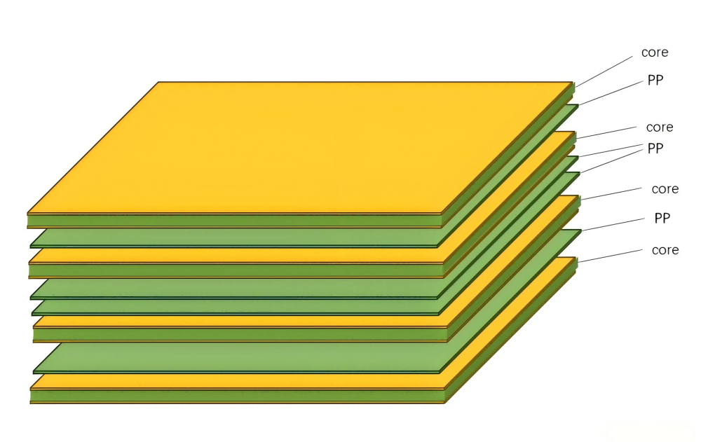
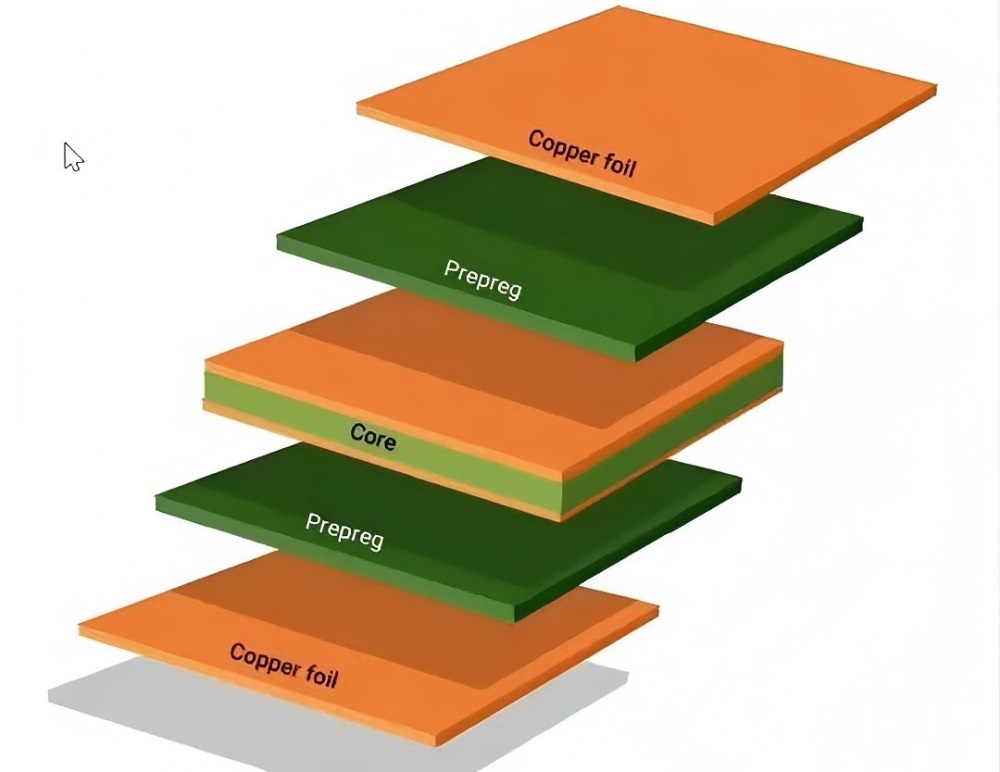
What is a PCB stackup?
A PCB stackup refers to the arrangement of copper layers and insulating layers that make up a PCB before the layout design. A PCB stackup helps minimise the circuit’s susceptibility to external noise, as well as minimise signal amplitude and reduce impedance and crosstalk issues in high-speed PCB layouts.
Types of PCB Layers
For multilayer PCBs, three main types of layers are used: signal layers, plane layers, and mixed layers. Signal layers consist of various types of signals.
- Signal Layers
Signal layers contain various types of signals and are not dependent on specific standards. They primarily carry low-voltage, low-current signals and are mainly used for transmitting medium- to high-speed data lines.
This type of layer does not include ground planes or power planes created by pouring copper. This is because, in very high-speed signals, the presence of ground or power planes can cause impedance variations due to the accumulation of stray capacitance and stray inductance.
- Ground Planes
Ground planes are distinct in that they contain no signals other than ground or power planes. They are primarily used to provide good ground and power paths throughout the circuit for various reasons. Solid copper is placed across the entire board; simply cutting through the copper plane creates separate segments to provide distinct signal planes.
- Hybrid Layer
This layer combines signal traces with copper fill to form a hybrid plane. It is the most common layer type in two-layer and six-layer boards, and is sometimes used in four-layer boards as well. Hybrid layers are found on standard PCBs that do not feature prominent high-speed traces.
Why Use PCB Layering?
Evolving Demands
As technology advances, the requirements for electronic products become increasingly stringent. There is a demand for PCBs that are smaller and lighter, while also offering better functionality, reliability, and a longer lifespan. This has led to the development of multilayer PCBs.
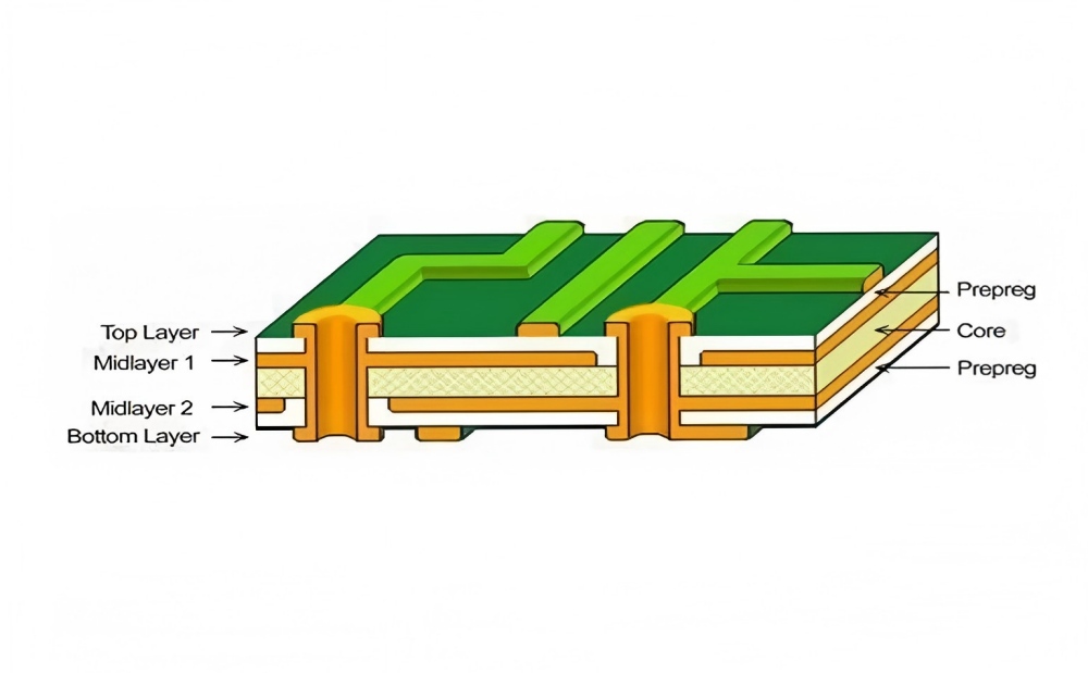
Multilayer PCBs are created by stacking two or more single-sided and/or double-sided PCBs together, with reliable, predefined interconnections between them. A multilayer PCB consists of three or more conductive layers, with two outer layers and an insulating layer in between. As PCB complexity and density increase, inefficient layer stacking designs can lead to issues such as noise, stray capacitance, and crosstalk.
PCB stacking is one of the most critical factors in determining EMC performance
PCB stackup is one of the most critical factors in determining a product’s electromagnetic compatibility (EMC) performance. A well-designed stackup can minimize radiation and protect circuits from interference by external noise sources. It can also reduce issues such as signal crosstalk and impedance mismatch.
However, a poorly designed stackup may lead to increased EMI (electromagnetic interference) radiation, as impedance mismatch causes reflections and ringing within the system, significantly degrading product performance and reliability.
PCB stack-up helps maintain signal integrity
PCB stackup can be designed to include features that help maintain signal integrity. Maximum capacitive decoupling in the power distribution network is achieved by placing the power plane directly adjacent to the ground plane in the stack-up. Signal layers or PCB layers should always have an adjacent ground plane within the PCB stack-up. Including a ground plane adjacent to each signal layer enhances flux cancellation and eliminates noise. Minimising the spacing between conductive PCB layers increases flux cancellation.
High-speed traces are best routed as striplines to maximise the shielding and flux cancellation provided by the adjacent ground layer. Less sensitive traces with a lower risk of air coupling should be routed on the outer layers of the printed circuit board. Further routing techniques involve combining the aspect ratio of chassis connections with ground pins between each layer. Ground fills between outer-layer traces with a large number of ground pins provide return paths and mitigate the generation of loop currents.
Avoid Discontinuities and Loops in PCB Layers
Use a layout that minimizes RF energy by avoiding unnecessary impedance and unnecessary materials, such as excessively thick copper. Design the PCB stackup to eliminate impedance buildup and divert RF energy to the chassis. Route signals to ensure return paths are directly beneath the signal traces. Avoid impedance loops on the PCB when fast-switching signals are present.
Evaluate PCB layers when placing buried vias to ensure there are no discontinuities. Discontinuities create gaps in the layer plane and may force return paths into noise-generating loops. Place decoupling capacitors on the power rails of each component to shunt switching signals to ground, and place bypass capacitors on switching signals at connectors entering and exiting the design.
PCB Stackup for Capacitive Decoupling and Magnetic Flux Cancellation
Arrange power and ground planes adjacent to each other to ensure clean power distribution across the entire PCB layer. When power and ground planes are adjacent in the stackup, low-impedance capacitive decoupling results in clean power distribution. Continue to ensure the integrity of the power distribution network across the entire layer by adding decoupling capacitors at the power leads of each component connected to the PCB layer.
Designing decoupling capacitors around each component’s power leads provides power to large digital networks that switch simultaneously. Adding decoupling capacitors at signal pins that undergo transitions during clock cycles ensures power distribution integrity across the entire layer. Decoupling and bypass capacitors provide sufficient power to maintain expected signals during operation, preventing ground bounce and the unintended injection of RF energy into the PCB layer.
Avoiding Unwanted Impedance and Loops
Stacking signal layers adjacent to ground layers prevents the formation of loops that generate RF energy. When the return plane is directly adjacent to the signal plane, no loop is formed. Via placement is critical for avoiding slots in the layer stack where signals may need to propagate around the slots, thereby creating loops. Additionally, high-speed signals generate flux in both the signal network and the return network.
This flux is equal and opposite between the signal and the return. Maximum cancellation occurs when high-speed signals and returns are placed directly adjacent to each other. The magnetic flux generated by high-speed signals must be eliminated to maintain electromagnetic compatibility (EMC). Design the PCB stackup to ensure that the return layer is adjacent to each signal layer, thereby achieving electromagnetic compatibility (EMC). EMC indicates that the stackup design is intended to properly minimize the generation of magnetic flux.
Differences Between Standard and HDI Stackups
PCB Stack-Up Design Rules
- Just like any other design or product manufacturing process, designers should follow certain rules to produce the highest-quality products. Therefore, designers must ensure they identify and adhere to proven PCB stack-up design best practices. For PCB stack-up design, several rules should be considered to achieve optimal results.
- The use of ground planes is highly recommended, as they enable signal routing within a stripline configuration. Furthermore, it plays a crucial role in reducing ground noise. Due to the reduced ground impedance, ground noise is significantly minimized.
- For high-speed signals, they must be routed on the intermediate layers located between different layers. In this way, the ground plane acts as a shield and contains radiation emitted from the traces at the highest speed.
- Even in adjacent planes, ensure that signal layers are very close to each other but that no two signal layers are adjacent.
- Signal layers must be close to the planes
- Ensure the stackup is symmetrical
- Efforts should be made to improve EMI performance and reduce noise
- The thickness of each signal layer must be considered
- Furthermore, it is important to consider the characteristics of the required materials. Pay attention to the thermal, electrical, and mechanical properties of such materials.
- Consider the software used when designing the stackup.
- For tight coupling, place signal layers close to the internal power layers
- There should be minimal space between the power layers and ground layers
Summary
The decision regarding how many layers to use in a design and the stacking method should be based on numerous factors, including the number of signal networks on the board, component density, pin density, signal frequency, and board size. These factors must be considered comprehensively. Designs with a larger number of signal networks, higher component density, greater pin density, and higher signal frequencies should, whenever possible, utilize a multilayer board design. To achieve good EMI performance, it is best to ensure that each signal layer has its own reference layer within the PCB stackup.