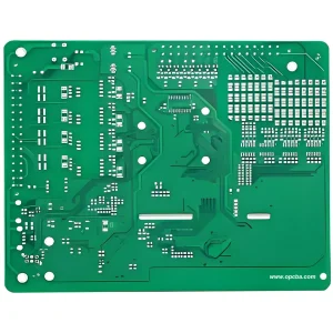
Half-hole PCB Product Description
The half-hole PCB is also called a castellated hole PCB. It has metallized half-holes on the board edge and supports connector-free board-to-board soldering. Moreover, it combines mechanical fixation and electrical connection in one structure. It is small, reliable, and easy for SMT assembly.Besides, it is widely used in high-density module products.
Structural Composition
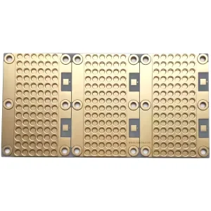
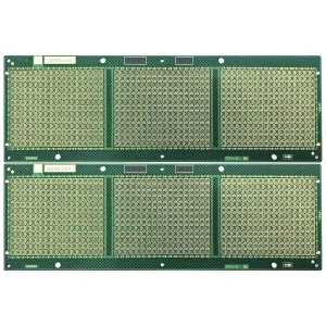
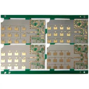
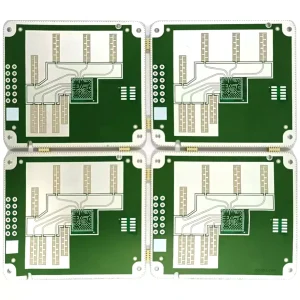
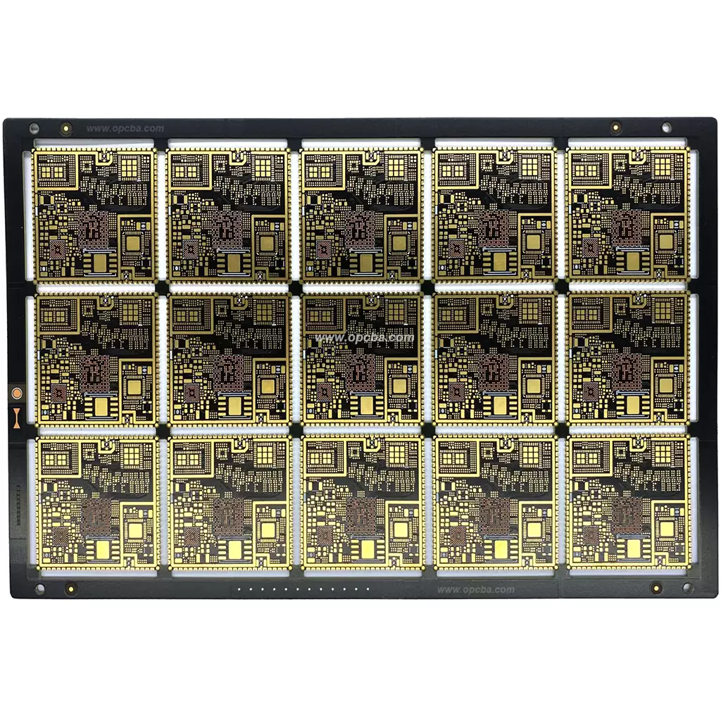
Substrate Material (Mainly FR-4)We use FR-4 as the main substrate material. In addition, we offer high-frequency and high-Tg materials as alternatives. This substrate delivers good heat resistance and insulation to ensure stable performance.Metallized Half-Hole Its half-holes come from fully plated through-holes. We cut them via precision CNC machining, and its copper layer is uniform and strongly adhesive. Therefore, it guarantees reliable soldering and stable electrical connection. Circuit Layer It supports single, double, multilayer and HDI PCBs. Besides, its fine line width and spacing enable stable routing. Surface Treatment (ENIG, HASL, OSP) Common surface finishes include ENIG, HASL, OSP, and more. They fit different soldering and reliability needs, and we can customize them as required. Shape and Precision Its board edges are smooth and burr-free. Moreover, its half-hole positions are highly accurate. Thus, it ensures high SMT assembly yield.
Key Design Considerations
Half-hole Size and Pitch
Its hole size, pitch and ring width follow strict standards. Besides, they avoid poor soldering or short circuits.
Line Width/Spacing and Layer Count Its line width and spacing can be 3–6 mils. In addition, its design follows current, impedance and signal needs.
Board Thickness Its typical thickness is 0.4–2.0 mm. It matches space, mechanical strength and heat dissipation needs, and we can adjust it according to requirements.
Hole Wall Copper Thickness and Adhesion Its copper thickness meets industry standards. Moreover, it has strong adhesion to prevent copper layer separation.
Application Areas
It is widely used in wireless communication modules, such as WiFi, Bluetooth and 5G modules. In addition, it applies to consumer electronics like TWS headphones and smart wearables. Moreover, it is suitable for industrial, automotive and medical electronic modules. Besides, it fits power and IoT modules for high-density interconnection.
This PCB is a customized product. Please send the Gerber file to our email: sales@opcba.com
We will provide you with a quotation as soon as possible.