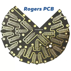
Ceramic PCB: When Heat, Frequency, and Reliability Leave No Room for Compromise
Standard FR-4 has a thermal conductivity around 0.3 W/m·K. Aluminum-backed boards push that to roughly 1-3 W/m·K. A Ceramic PCB built on aluminum oxide starts at 20 W/m·K. One built on aluminum nitride can exceed 170 W/m·K.
That two-order-of-magnitude difference isn’t an incremental improvement. It’s what makes the difference between a power module that needs active cooling and one that can dump its heat passively into a chassis. Between an RF amplifier that drifts as it warms up and one that holds its bias point stable. Between an LED array that degrades after 5,000 hours and one that maintains 80% lumen output past 50,000.
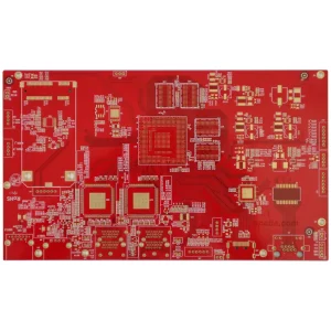
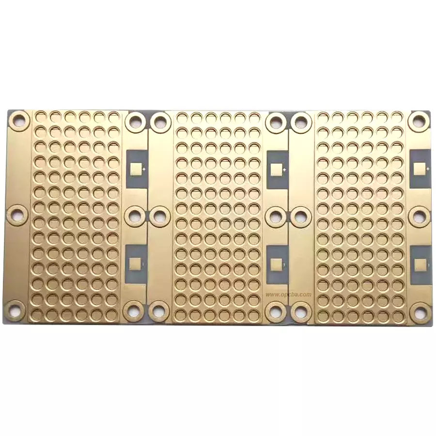
We fabricate alumina ceramic PCB and aluminum nitride PCB products from single-sided to 12-layer designs. The ceramic substrate is the foundation. Everything else—copper thickness, surface finish, via structure, metallization method—is chosen to match what that substrate can do. For full parameter and application details of the most widely used substrate, check our dedicated guide: Alumina ceramic PCB
Two Ceramics, Two Performance Classes
The choice of ceramic material sets the thermal and mechanical envelope for the entire design.
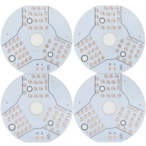
Alumina (Al₂O₃) is the established workhorse. Thermal conductivity of 20-30 W/m·K. Coefficient of thermal expansion around 7-8 ppm/°C—close enough to silicon and gallium arsenide to manage die-attach stress in most applications. Dielectric strength above 15 kV/mm. The material is widely available, the processing is mature, and the cost is predictable. For power LED modules, DC-DC converters, ignition circuits, and most industrial power applications, alumina does the job at the lowest cost in the ceramic category.
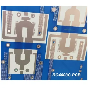
Aluminum Nitride (AlN) moves into a different performance class. Thermal conductivity of 170-200 W/m·K—comparable to some metals. CTE of 4-5 ppm/°C, nearly matching silicon. Dielectric constant around 8.8 at 1 MHz. These numbers matter when you’re packing hundreds of watts into a module the size of a postage stamp, or when you’re running an RF power amplifier where every degree of temperature rise shifts the gain and phase. AlN costs more—significantly more—but for high-power laser diodes, aerospace motor drives, and base station power amplifiers, the thermal margin it provides is the difference between a design that works and one that requires a complete thermal rethink.
I’ve seen a team switch from alumina to AlN on a compact motor controller and eliminate a dedicated cooling fan from the BOM. The substrate cost went up. The system cost went down. That’s the trade-off worth calculating.
What You Can Specify
Our standard Ceramic PCB capability covers the following range:
-
Board thickness: 0.25 mm to 4.0 mm. At the thin end, substrates as thin as 0.25 mm are used in RF and microwave applications where low profile and short thermal path matter. At 4.0 mm, the ceramic provides structural rigidity for large-format modules and can accommodate deep laser-drilled vias.
-
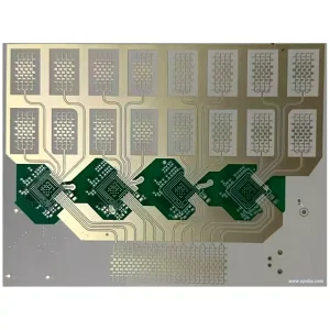
Layer count: 1 to 12 layers. Single-layer ceramic boards are common in LED and simple power applications. Multilayer stacks—using either high-temperature co-fired ceramic (HTCC) or low-temperature co-fired ceramic (LTCC) processes—support complex routing with embedded passives and buried cavities. Above four layers, the process shifts from direct-bonded copper (DBC) to co-fired technologies, which changes the via metallization and the conductor material options.
-
Copper weight: 0.5 oz to 4 oz. Thin copper suits fine-pitch RF traces; thick copper handles high-current power paths. For a given trace width and temperature rise, 4 oz copper carries roughly four times the current of 1 oz. On a ceramic substrate, the limiting factor is usually the adhesion strength between the copper and the ceramic—not the copper itself.
-
Minimum trace/space: 2 mil. This is the floor for our ceramic processing. At this dimension, the metallization method (sputtered seed layer followed by electroplating vs. DBC lamination) becomes a critical process decision that affects both resolution and adhesion.
-
Solder mask: Black, transparent, or green. Black is used when the board is visible and needs to disappear into the product. Transparent is chosen for optical applications or when the ceramic substrate’s natural white appearance is part of the product aesthetic. Green is available for visual consistency with standard PCB assemblies.
-
Silk screen: White or black, selected for legibility against the chosen solder mask.
-
Surface finish: Immersion gold (ENIG), immersion silver, or plated gold. Plated gold is common on alumina ceramic PCB products used in wire-bonding applications—it provides a surface that aluminum or gold bond wires can reliably attach to. ENIG and immersion silver are used for standard SMT assembly and offer good shelf life and solderability.
Design Considerations for Ceramic
Laser-drilled vias are standard. Mechanical drilling causes micro-cracks in ceramic that propagate under thermal cycling. We use laser drilling for all ceramic via formation. This limits the maximum via diameter compared to mechanical drilling but ensures structural integrity.
Via metallization differs from FR-4. Ceramic vias are filled with a conductive paste (in HTCC/LTCC processes) or electroplated copper (in DPC processes). The via resistance in co-fired ceramics is higher than a plated copper via in FR-4. If your design has high-current paths through vias, factor this into your voltage drop calculations.
Coefficient of thermal expansion matching. One of the strongest arguments for aluminum nitride PCB in power modules is CTE compatibility. Silicon dies, wide-bandgap semiconductors (SiC, GaN), and AlN all sit in the 3-5 ppm/°C range. Directly bonding a die to an AlN substrate minimizes the shear stress on the die-attach layer during thermal cycling. This is why AlN is the substrate of choice in high-reliability power modules for aerospace and automotive traction inverters.
Brittleness. Ceramic does not bend. It fractures. Mechanical mounting requires even pressure distribution—point loads from uneven standoffs or over-torqued screws will crack the substrate. If the board is large (above 50 mm × 50 mm), we recommend a mounting frame or a compliant thermal interface layer rather than rigid standoffs at the corners.
Applications
Ceramic PCB products are used wherever the substrate itself must solve a thermal or high-frequency problem that FR-4, metal-core, and polyimide cannot. The core markets are high-power LED and laser diode modules, automotive engine-bay electronics and traction inverters, aerospace power distribution and motor drives, medical imaging and implantable devices, and RF communication equipment including base station power amplifiers, antenna modules, and microwave backhaul transceivers.
Ordering
This is a custom product. Every alumina ceramic PCB or aluminum nitride PCB we build is defined by the application’s thermal budget, frequency requirements, and mechanical constraints—not by a stock configuration.
To get a quotation, send your Gerber file and stackup requirements to sales@opcba.com. Include your preferred ceramic material, surface finish, copper weight, and target quantity. We’ll return a formal quote with a lead time as soon as the engineering review is complete.