Electrical Performance for PCB: Overview of Halogen-Free PCB
Halogen-Free PCB is an eco-friendly printed circuit board. It strictly controls halogen (Cl, Br) content. It uses phosphorus/nitrogen-based flame retardants instead of traditional ones. It also complies with RoHS, IEC and other global environmental regulations.
Core Definition and Compliance
Halogen-Free PCB is not absolutely halogen-free. Instead, it keeps Cl, Br and total halogen within industry limits. Specifically, it meets IEC 61249‑2‑21 and JPCA‑ES‑01‑2003 standards (Cl, Br ≤ 900 ppm; total halogens ≤ 1500 ppm). High-end enterprises set stricter requirements (Cl, Br ≤ 600 ppm). Additionally, manufacturers mark products with “Halogen‑Free”. They test them through SGS/TÜV/CTI. They also ensure they meet RoHS, REACH and WEEE standards.
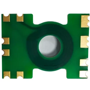
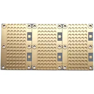
Material System and Core Characteristics
It adopts a halogen-free flame-retardant system (phosphorus-based, nitrogen-based, inorganic). This system meets UL94 V-0 standards. Moreover, its main substrates include high Tg FR-4 (for consumer electronics). It also includes modified epoxy (for 5G), PPE/PPO (for high-frequency devices) and BT resin (for high-reliability equipment).
Key Performance Advantages
Compared with traditional halogen-containing PCBs, it has key advantages. First, it is eco-friendly and safe. It releases no toxic gases. Second, it is heat-resistant and reliable. It has a higher Tg and stable performance. Third, it is electrically adaptable. It fits high-frequency/high-voltage scenarios. Finally, it is process-compatible. It requires no major equipment modification.
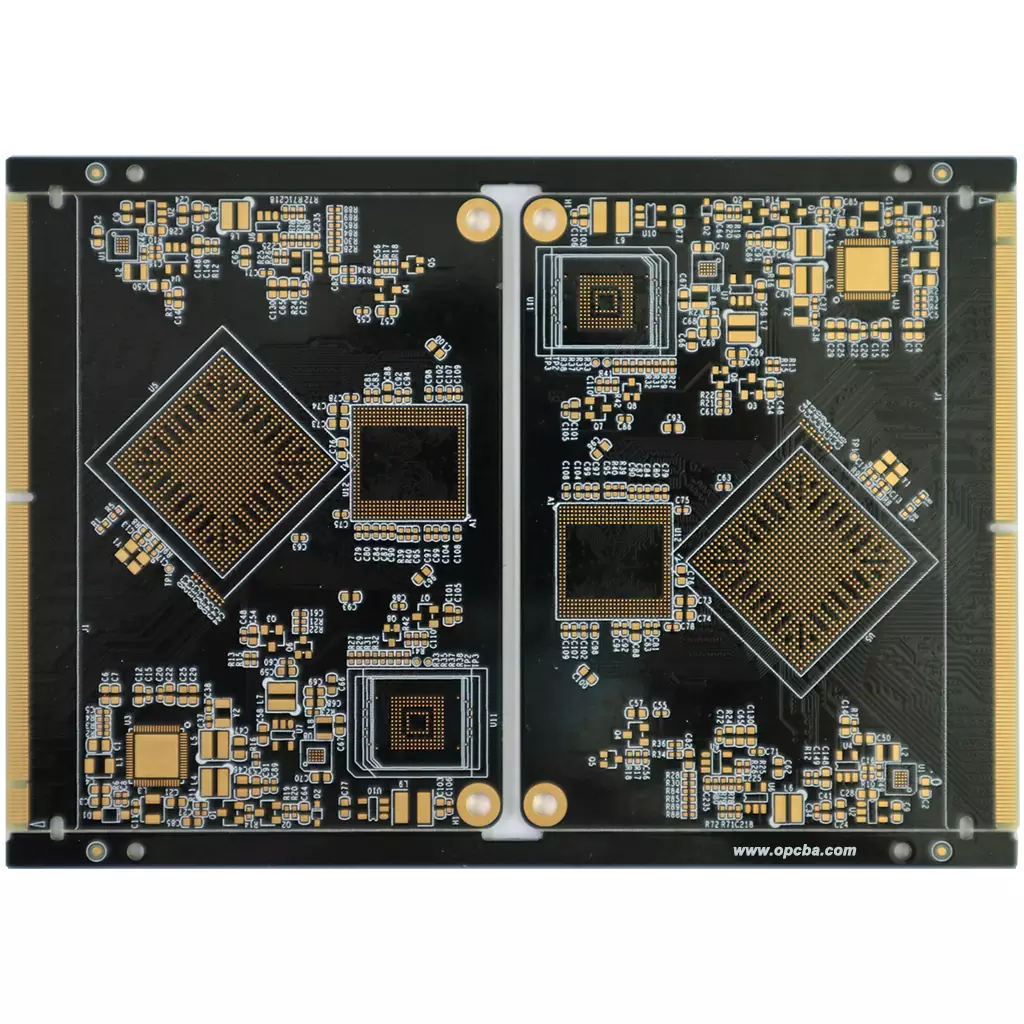
Full-Process Control and Applications
Manufacturers implement strict full-process control. This ensures halogen compliance. Control ranges from raw material testing to finished product inspection. As a result, it is widely used in many fields. These include consumer electronics, automotive electronics, communications, medical equipment, aerospace and new energy.
Advantage Summary
In summary, Halogen-Free PCB has key features. It meets environmental standards, is safe and high-performing. It helps avoid export risks. It enhances device reliability. Thus, it becomes a key choice for green and high-end electronic upgrades.