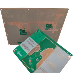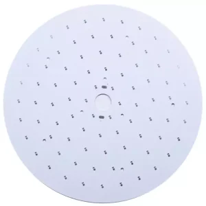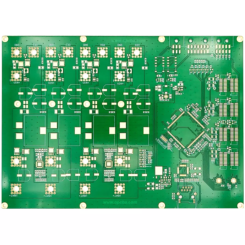
Product Overview of Heavy Copper PCB
Heavy Copper PCB is engineered for ultra-high current carrying capacity and exceptional thermal stability. Unlike standard PCBs, it uses ultra-thick copper layers to minimize resistance and heat buildup drastically. Consequently, it perfectly meets the core power distribution demand of modern high-power electronic systems.
It is a specialized branch of printed circuit board technology. For this reason, you can explore the full spectrum of PCB types and manufacturing fundamentals at https://opcba.com/pcb/. Moreover, heavy copper circuit boards power industrial power supplies, automotive BMS, and aerospace systems with reliable current handling.
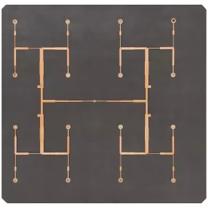
Structural Composition of Heavy Copper PCB
Every Heavy Copper PCB has a robust structure optimized for high-power performance. Above all, each component plays a critical role in preserving power integrity.
Ultra-thick copper layers carry high-current power. Specifically, their thickness eliminates voltage drop and hotspots for stable operation. In contrast, dielectric layers provide electrical isolation—high-temperature materials are mandatory here.
Ground and power planes offer stable power distribution and heat dissipation. Simultaneously, they actively cut down thermal stress for heavy copper traces. Additionally, the substrate has reinforced mechanical strength. This means it enables reliable mounting for heavy components, a must for high-power designs.
Key Design Considerations for Heavy Copper PCB
Designing a Heavy Copper PCB demands focus on critical engineering factors. In fact, each directly impacts power performance and reliability.
Current capacity calculation is non-negotiable. To achieve this, designers calibrate copper thickness and trace width to match target values. As a result, this prevents overheating and component failure. Thermal management needs strict layout rules: short power paths, dedicated heat sinks, and thermal vias. For example, these steps minimize thermal resistance and ensure safe operation.
Manufacturing compatibility relies on specialized etching and plating processes. Thus, this ensures uniform copper thickness and structural integrity. Mechanical stability is vital too. Since heavy copper boards carry heavy components, reinforced substrates boost longevity.
Ultimately, align designs with modern power distribution standards. For further insights, learn about the latest SMT equipment trends at https://opcba.com/2026-global-high-speed-smt-equipment-market-analysis/.
Material Selection for Heavy Copper PCB
A Heavy Copper PCB’s performance depends entirely on smart material choices. Essentially, every selection targets high-power and thermal needs.
Copper layers use high-conductivity, ultra-thick copper foils. For instance, these cut resistance and heat generation at extreme currents. Dielectric substrates use high-temperature laminates like FR-4 with Tg > 170°C. Likewise, they withstand thermal stress and maintain electrical isolation.
Laminate structures favor multi-layer designs with thick ground/power planes. Furthermore, this enhances heat dissipation and power distribution capabilities. Surface treatments like ENIG or hard gold plating protect copper traces. Also, they ensure reliable soldering and corrosion resistance.
Application Areas of Heavy Copper PCB
Heavy Copper PCB is irreplaceable for reliable power distribution across high-power industries. Clearly, its current handling capacity sets it apart from standard boards.
In industrial power supplies, converters and inverters use it for high-current power handling. As a result, this powers heavy machinery and industrial automation. In automotive systems, BMS and PDUs rely on it for battery power distribution. Therefore, it enables safe and efficient electric vehicle operation.
In aerospace electronics, it enables stable power distribution for satellite systems. Notably, this is critical for mission-critical operations. In renewable energy, it supports solar inverters and wind turbine controls.
In battery management systems, it delivers ultra-stable power paths. Even so, extreme charging/discharging cycles won’t compromise its performance in energy storage systems.