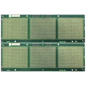
2-layer PCB is a printed circuit board with copper foil conductive layers covering both sides and electrically connected through metalized vias.
2-layer PCB provides higher wiring density and design flexibility than a single-sided PCB board within a limited board area, while also having lower manufacturing costs compared to a multi-layer PCB board, thus achieving a good balance between cost-effectiveness and complexity.
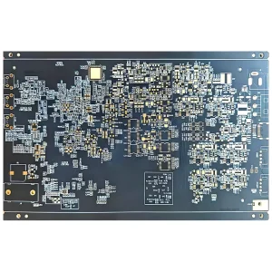
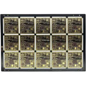
The core of 2-layer PCB manufacturing lies in the hole metallization process to ensure reliable interconnection between layers. The 2-layer PCB type is widely used in fields such as consumer electronics, communication equipment, industrial control, and automotive electronics, and is one of the most mainstream choices in modern electronic hardware design.
The difference between 2-layer PCB and 1-layer-PCB is that the circuit of a single-sided PCB is only on one side of the PCB board, while the circuit of a double-layer PCB can be connected to the double-sided PCB board circuit on both sides of the PCB board through a through-hole in the middle
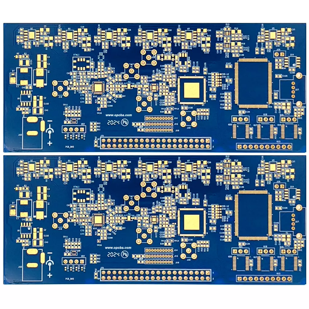
The manufacturing process of 2-layer PCB involves key steps such as substrate preparation, drilling, hole metallization, pattern transfer, etching, solder mask and screen printing, surface treatment, testing, and board splitting. The preparation of the substrate usually uses FR-4 glass fiber substrate, double-sided laminated copper foil. Drill through holes and positioning holes using CNC drilling machines.
Hole metallization involves depositing a conductive layer on the hole wall through chemical copper deposition and electroplating, achieving interlayer interconnection, which is a key step in determining the reliability of double-sided panels. Pattern transfer involves double-sided coating with photoresist, exposure, and development to form an anti etching layer for circuit patterns. Etch and corrode the copper foil in the unprotected area, while preserving the circuit pattern.
Solder mask and screen printing involve coating solder mask ink to prevent oxidation and insulation, and adding screen printing to identify component part numbers. Surface treatment options include tin spraying (HASL), immersion gold (ENIG), OSP, and other processes to enhance pad solderability. Finally, perform on/off testing and board splitting.
The finished thickness of 2-layer PCB can be customized according to design requirements, with the most common standard thickness being 1.6mm. Other common optional thicknesses include 0.8mm, 1.0mm, 1.2mm, 2.0mm, etc. The typical production range is approximately between 0.4mm and 3.2mm.
The most commonly used core substrate for 2-layer PCBs is FR-4 (epoxy glass cloth laminated board), which has good mechanical strength, electrical insulation, heat resistance, and cost-effectiveness. According to special application requirements, other materials can also be selected, such as aluminum substrates (metal substrates) for high heat dissipation scenarios; High frequency materials such as polytetrafluoroethylene (PTFE) are used in high-frequency circuits such as 5G/RF.
Flexible 2-layer PCB (polyimide) is used for flexible circuit boards (FPC); Ceramic substrates are used in extreme environments such as high power or high frequency. To protect the solder pads and enhance solderability, common surface treatment processes include tin spraying (HASL), immersion gold (ENIG), and oxidation protection (OSP), each with different solderability, flatness, and cost characteristics.
In the design of 2-layer PCB, the via size needs to be considered. The standard via hole diameter is usually 0.3-0.5mm, and the pad diameter is 0.6-0.8mm. For high-density design, vias with a hole diameter of 0.2-0.3mm can be used; The diameter of the power/grounding via can be increased to 0.5-0.8mm to carry high currents or assist in heat dissipation; When designing, attention should be paid to the plate thickness aperture ratio (recommended ≤ 8:1) and the minimum process limit.
According to the different substrate materials, 2-layer PCB boards can be mainly divided into the following types:
FR-4 PCB board, the most widely used and economical type, suitable for the vast majority of consumer electronics, industrial control, and communication equipment.
Aluminum substrate (metal substrate), with aluminum plate as the heat dissipation core, has excellent thermal conductivity and is widely used in fields such as LED lighting and power modules that require efficient heat dissipation.
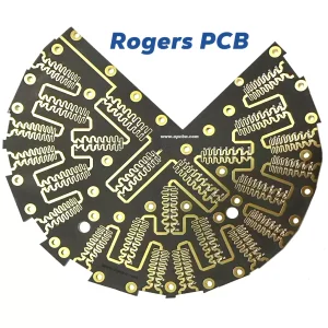
High frequency 2-layer PCB, made of low loss materials such as polytetrafluoroethylene (PTFE) or modified epoxy resin, with stable dielectric constant and low signal loss, specially designed for high-frequency and high-speed circuits such as 5G, radar, RF, etc.
Flexible 2-layer PCB with polyimide (PI) substrate, bendable and foldable, used for designs such as mobile phone cables, wearable devices that require dynamic bending or save three-dimensional space.
2-layer ceramic substrate with extremely high thermal conductivity and stability, used in special fields with high power density or high reliability requirements, but at a higher cost.
With the increasing demand for miniaturization of devices, 2-layer PCB forward high-density interconnect (HDI) technology has evolved, using laser micro holes (aperture ≤ 0.1mm) instead of mechanical drilling to achieve finer wiring. By using processes such as overlaying local buried blind holes, a 2-layer PCB board can achieve performance similar to a multi-layer board, while increasing costs by only 15% to 30%. With mature technology, reliable performance, and excellent cost control, 2-layer PCBs will continue to dominate the mainstream of electronic hardware design in the foreseeable future.