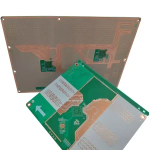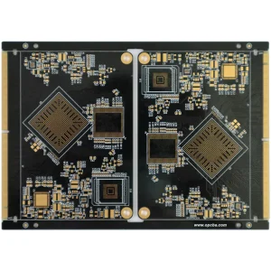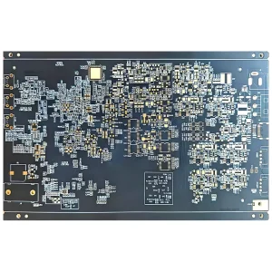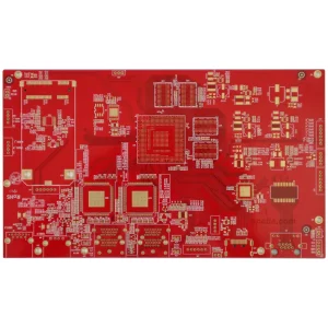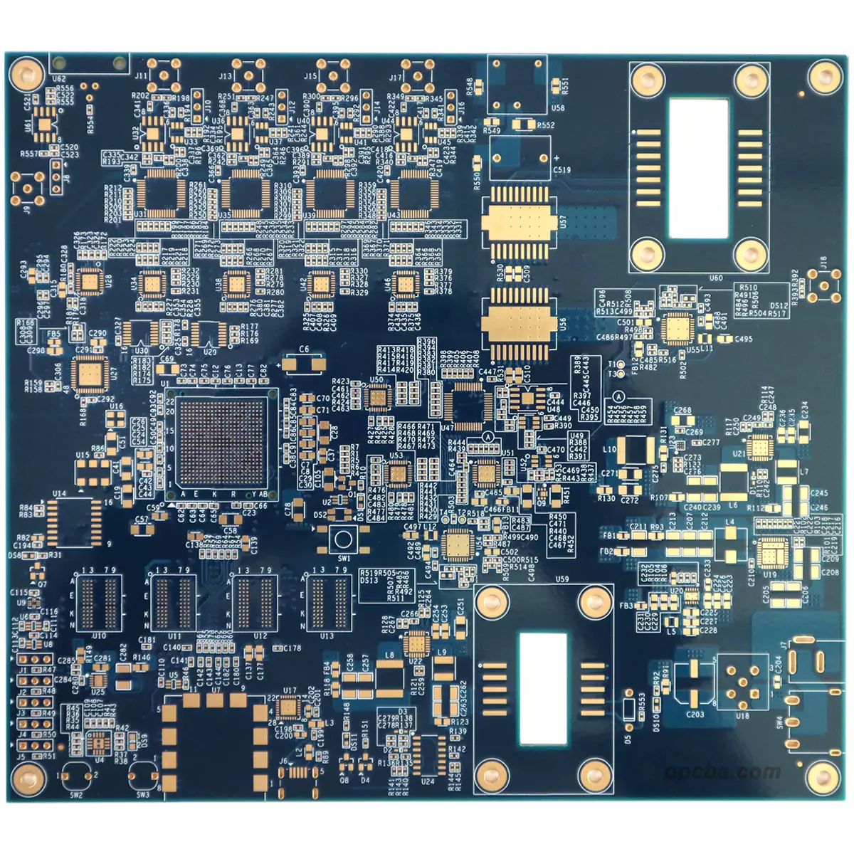
Overview of 8-Layer PCB
An 8-layer PCB costs noticeably more than a six-layer board, and the extra spend buys a second plane pair plus a cleaner reference scheme. Designs land here when high-speed interfaces need controlled impedance on several layers at once, or when the number of supply rails outgrows a single plane pair.
Structural Composition
A typical eight-layer stack alternates signal and plane layers around the center: signal, ground, signal, power, power, signal, ground, signal. Two plane pairs let ground and power each keep a dedicated reference layer, which is the main electrical gain over six layers.
The build needs thinner cores and an extra press cycle. Registration gets tighter and the laminator has to hold alignment across more material, which is where much of the process cost sits. Our PCB construction page covers how those layers are bonded and drilled.
Key Design Considerations
Eight layers add layout options, and the plan has to account for them from the start.
- Controlled impedance applies per layer. Differential pairs at 90 or 100 Ω and single-ended traces at 50 Ω can share one board, so the stack-up is defined before routing begins.
- Plane splits and return paths matter more. With high-speed nets on several layers, a split plane forces return current to detour, and that shows up as radiated noise.
- Via structure becomes a real choice. Through-hole vias are the cheapest option; blind and buried vias cost more but free routing area on dense inner layers.
- Lamination cycles set the schedule. Each sequential press adds process time, and alignment tolerance accumulates with it.
Multi-Field Applications
Eight layers appear where wiring density and signal speed rise together:
- Networking and telecom: base station boards, switches, and high-speed data equipment.
- Computing: motherboards, expansion cards, and memory modules needing several controlled-impedance layers.
- Industrial control: multi-axis controllers and data acquisition cards.
- Automotive: engine control units and infotainment platforms.
Material Selection & Cost Reference
The substrate and the stack-up get chosen together at this layer count. A high-speed design usually drives the move to a low-loss laminate, and the dielectric thickness that laminate allows is what sets the impedance targets above.
An eight-layer board runs about 2.2 to 2.8 times a comparable four-layer board, and roughly 40 to 60 percent above a six-layer one. Two things drive the gap: the extra lamination cycle and the thinner cores the stack requires. Drilling adds its share too, since via aspect ratio limits start pushing designs toward blind or buried vias.
At this layer count, material is typically 25 to 35 percent of total cost, lamination 15 to 25 percent, and drilling 10 to 20 percent. Yield loss stays modest at eight layers and becomes a major line item at twelve and above.
The multipliers above reflect published 2026 China-manufacturer quotes for standard FR-4 multilayer boards.