RF radio frequency PCBA Product Description
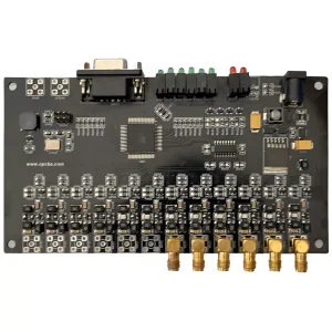
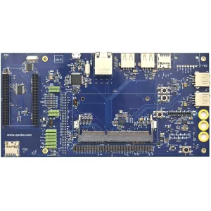
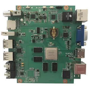
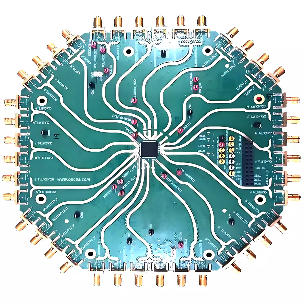
RF Radio Frequency PCBA is a precision-engineered electronic assembly designed for high-frequency signal transmission and processing. It integrates RF-grade components on specialized low-loss substrates, delivering stable, low-interference performance for wireless systems. This assembly is the core of radar, 5G communication, and automotive RF modules, directly determining the accuracy and reliability of signal detection, data transfer, and real-time processing.
Definition and Role RF radio frequency PCBA
- Full Name and Essence: RF Radio Frequency PCBA is a precision assembly tuned for signal integrity. It excels in ultra-high frequency scenarios, from automotive sensing to long-range communication.
- Difference from General PCBA: General PCBA focuses on low-frequency power flow. Conversely, this high-frequency assembly prioritizes impedance control to eliminate signal loss and electromagnetic crosstalk.
- Core Value: It acts as the “signal brain” of high-frequency devices. Without it, radar detection and wireless data transfer would lack the precision modern industries demand.
Key Assembly Components
- Basic Carrier: High-frequency PCBs made from low-loss substrates form the base. These boards keep signal attenuation to a minimum. For automotive-grade PCB insights, visit https://opcba.com/mall/automotive-pcba/.
- Active & Passive Parts: Engineers select RF-qualified chips, sensors, and connectors for these assemblies. Each component is tested for anti-interference in dense signal environments.
- Performance Materials: High-frequency solder paste and shielding films are integral. Additionally, low-loss adhesives lock in components for long-term stability.
Materials and specifications
Substrate choice sets the ceiling on RF performance. We build on low-loss laminates including Rogers RO4000 and RO3000 series, Taconic TLX and TLY series, and Wangling PTFE grades. Where cost matters more than marginal loss, we laminate RF material against FR-4 in hybrid stacks and keep the signal layers on the premium sheet. Standard limits for these builds are published on our capability sheet; the figures below cover typical RF PCBA orders.
| Layers | 2 to 8 (typical radar and RF module builds) |
| Minimum trace / space | 3 mil on 18 um base copper |
| Impedance tolerance | +/-5 ohm below 50 ohm; +/-10% at 50 ohm and above (+/-5% on review) |
| Laser via | 0.10 mm |
| Surface finish | ENIG, OSP, immersion silver or tin; selective finishes available |
Confirm the exact limits for your stack-up with our engineering team before release, since copper weight and material grade move these numbers.
RF radio frequency PCBA Precision Production Workflow
This high-frequency assembly follows a strict, step-by-step manufacturing process:
- PCB Validation: Engineers screen high-frequency PCBs for impedance accuracy and surface quality to eliminate early-stage flaws.
- Component Prep: Teams verify part models first. Then, they sort materials by batch to maintain full production traceability.
- Solder Paste Deposition: Technicians apply high-frequency solder paste to pads with micron-level thickness control.
- Component Placement: High-precision machines mount miniaturized RF parts onto designated pads with tight tolerance limits.
- Controlled Reflow: A custom temperature curve melts the solder paste, safeguarding sensitive RF chips while forming strong joints.
- Connector Integration: Specialists manually solder RF connectors and add anti-vibration reinforcement for rugged use.
- Cleanup & Correction: Technicians remove flux residues thoroughly. They also fix minor defects like cold solder joints right away.
- Functional Testing: Inspectors run RF performance checks on finished units. Finally, they package validated assemblies in anti-static, moisture-proof casings.
RF radio frequency PCBA Primary Application Sectors
This high-frequency assembly powers critical systems across industries:
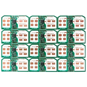
- Millimeter Wave Radar: It enables precise target detection for ADAS and industrial sensing. For deep dives into radar tech, see https://opcba.com/millimeter-wave-radar/.
- Automotive RF Systems: It supports tire pressure monitoring and in-vehicle communication, thriving in extreme temperature and vibration conditions.
- 5G Infrastructure: It facilitates high-speed signal transfer in base stations, making 5G’s low-latency promise a reality.
- Aerospace & Defense: It withstands harsh conditions in satellite communication and military radar, ensuring unbroken signal links.
- Wireless IoT: It shrinks high-frequency modules for wearables and industrial sensors, enabling efficient low-power data transmission.