In hardware design, RF antenna design is quite demanding. Besides performance, cost must also be considered, so antenna selection requires comprehensive considerations. A common low-cost approach is a PCB-mounted antenna. For 2.4 GHz applications, most PCB antennas fall into a small number of structures, and the two printed ones below cover the majority of low-cost designs.
Planar Inverted-F Antenna Design
For RF, any copper foil or wire cannot be considered a simple wire; it is an equivalent circuit composed of many resistors and capacitors. What reads as a short on a multimeter is not a short at RF. The key points for laying out an inverted-F antenna follow, with the figure below as the reference:
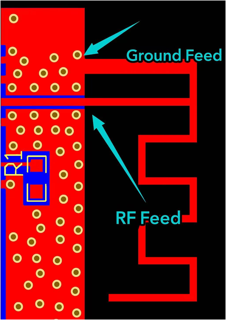
- The geometry is not freehand. Start from the antenna symbol in the component library, then set the arm length and the feed position, because those two dimensions fix the resonant frequency and the match.
- The impedance of the trace leading out of the RF feed point must be 50 ohms.
- The ground feed point must be securely grounded.
- The ground plane must have multiple ground vias, as shown in the figure above.
- The copper foil on all layers around the antenna must be clear.
- The antenna must be placed in a corner of the PCB board, ideally with three sides clear.
Two dimensions decide whether the antenna works: arm length and clearance. At 2.4 GHz the free-space quarter wavelength is about 31 mm, and a printed inverted-F on FR-4 comes out shorter than that because the laminate loads the antenna; the final length is set in simulation and trimmed on the first prototype. Clearance matters as much. Any copper inside the keep-out area, whether a ground pour, a trace or a via, detunes the antenna and costs efficiency, and unlike a length error it cannot be trimmed back afterwards.
Inverted-F Antenna Design for Bluetooth
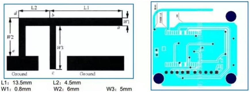
The antenna body of an inverted-F antenna can be linear or sheet-shaped. A laminate with a higher dielectric constant also reduces the size of the Bluetooth antenna, at some cost in bandwidth and radiation efficiency.
As a type of board-mounted antenna, the inverted-F antenna design offers low cost but increases size. It is the most common design in practical applications.
The antenna is typically placed on the top layer of the PCB, with the ground plane typically placed on the top layer near the antenna. However, the antenna must be free of ground and surrounded by clear space. See the figure below:
Inverted-L-Shaped PCB Board-Mounted Antenna Design
There are many PCB board-mounted antennas on the market, primarily the types shown in the figure below.
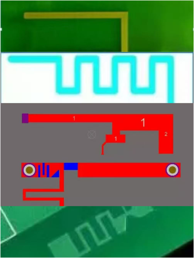
The inverted-L is the simpler of the two. A quarter-wave arm runs along the board edge and is fed at the short leg. With no shorting pin it takes less board area than an inverted-F of the same length, and its bandwidth is narrower, so it tolerates less copper near the arm.
In RF hardware development, selecting the correct PCB board-mounted antenna is only the first step in achieving optimal wireless performance. The RF antenna serves as the “signal output,” but it is the RF PCB that acts as the “highway” transporting those signals. If the PCB is poorly designed, particularly in ground plane integrity and via placement, the result can be signal loss, interference, impedance mismatch, or even total communication failure.
The last discontinuity on that highway sits at the board edge, where the trace meets an RF connector.
RF PCB Design Rules
Ground Plane Design for Microwave RF Boards
- The ground plane, which serves as the mirror image return path for RF signal lines, must be complete and independently defined, with no other signal lines routed on the ground plane;
- Unless it can be ensured that current will not form a loop on the ground plane, the ground plane should not be divided;
- For high-density boards, such as those using CSP packaging, dual-layer boards are not recommended. Use a four-layer RF construction instead, built on high-frequency hybrid laminates rather than on a standard FR-4 stack-up;
- The ground plane beneath RF signal lines should be as wide as possible. Narrow ground planes can cause parasitic parameters and increase attenuation;
- The ground plane and the top layer ground should be connected via vias between the two layers. It is essential to ensure that RF signal lines are fully “shielded” to enhance the product’s EMC performance;
- For the blank areas on the Top Layer and Bottom Layer, it is recommended to apply a ground plane and connect all ground areas via vias with a spacing no greater than λ/20;
- It is also recommended to wrap the power plane with ground vias to avoid unnecessary electromagnetic radiation.
The power plane also has to respect the “20H” principle against the ground plane. The rule requires the edge of the power plane to sit at least 20 times the plane separation inside the edge of the ground plane (the 0 V reference plane), where H is the dielectric thickness between the two planes. At 20H, about 70% of the edge field is contained under the ground plane instead of radiating out of the board edge. Pushing the inset to 100H raises that containment to roughly 98%, but it costs a wide strip of board area, so most designs stop at 20H or at a fixed inset of about 1 mm.
RF Board Via Design
At 2.4 GHz a wavelength in free space is about 125 mm, so λ/20 works out to roughly 6 mm. That number, rather than the general advice to use as many vias as possible, is what sets stitching pitch around an RF section.
- Use as many vias as possible to connect different layers, with intervals no greater than λ/20 of the signal wavelength;
- “Ground via accompaniment”: place as many vias as possible near signal lines to reduce via parasitic inductance;
- Avoid RF signals crossing layers as much as possible;
- Avoid sharing vias between pads and solder joints; keep them independent as much as possible;
- Use ground vias to isolate interference sources from sensitive circuits;
- For QFN-packaged devices, use as many vias as possible on the bottom pads;
Ultimately, RF PCB design and RF antenna design are inseparable. Even the most advanced antenna will underperform if the PCB layout fails to provide a clean, low-loss environment for RF signals. Ground plane integrity and via placement decide how much of the performance the antenna was designed for actually reaches the product. Get those two right and the impedance stays where the simulation put it, the emissions stay inside the limit, and the radio behaves the same on every unit that comes off the line.