Electronic component packaging is a critical foundation of reliable PCB design, directly impacting performance, thermal management, and manufacturing efficiency. As semiconductor technology evolves, packaging forms are rapidly advancing—from traditional through-hole designs to high-density surface-mount solutions. This article shares 8 expert tips for selecting and working with electronic component packaging, alongside a detailed breakdown of the most common package types and their applications.
1. Understand Core Packaging Categories
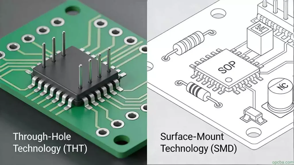
The packaging of electronic components is broadly divided into through-hole (THT) and surface-mount (SMD/SMT) technologies, each with distinct advantages:
- Through-Hole (THT): Pins insert through the PCB, offering high mechanical stability. Ideal for high-voltage, high-power applications (e.g., industrial control circuits).
- Surface-Mount (SMD/SMT): Components mount directly to the PCB surface, enabling miniaturization and automated assembly. Dominates modern consumer electronics, IoT devices, and high-density PCBs.
SMD component packaging, in particular, encompasses a vast range of standardized and evolving forms—including chip resistors, capacitors, and advanced IC packages like BGA and Flip Chip. While many passive components (e.g., resistors, capacitors) follow industry-wide standards, IC packaging continues to innovate to meet demands for higher I/O density and thermal performance.
2. Key Package Types & Their Applications
2.1 SOP/SOIC Package: Versatile Surface-Mount Standard
SOP (Small Outline Package) was pioneered by Philips between 1968–1969, and remains one of the most widely used surface-mount packages. Its compact, gull-wing pin design balances density and ease of assembly, making it suitable for low-to-medium I/O ICs (e.g., logic gates, amplifiers).
- Derivatives: SOJ (J-pin for high-vibration environments), TSOP (thin profile for memory chips), SSOP (reduced pitch for higher density), and SOIC (integrated circuit variant).
- Best For: Consumer electronics, automotive control modules, and low-power industrial devices.
2.2 DIP Package: Traditional Through-Hole Reliability
DIP (Dual In-line Package) is the classic through-hole package, with pins extending from both sides of a plastic or ceramic body. Its robust design and easy manual soldering made it ubiquitous in early electronics, and it remains relevant for high-reliability applications.
- Key Use Cases: Standard logic ICs, legacy memory modules, and industrial power circuits where mechanical stability is critical.
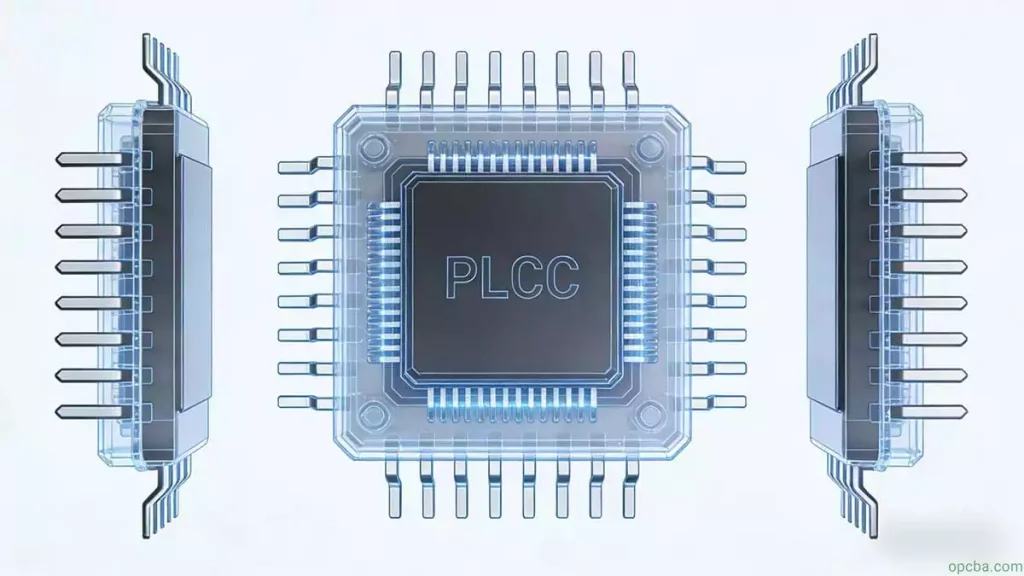
2.3 PLCC Package: High-Density Surface-Mount for ICs
PLCC (Plastic Leaded Chip Carrier) features a square body with J-shaped pins around all four sides, offering higher I/O density than DIP while retaining compatibility with SMT assembly. Its small footprint and reliable solder joints make it ideal for space-constrained PCBs.
- Best For: Mid-range ICs, microcontrollers, and communication modules in automotive and aerospace systems.
2.4 TQFP & PQFP Packages: High-I/O Flat-Pack Solutions
TQFP (Thin Quad Flat Package) and PQFP (Plastic Quad Flat Package) are flat, four-sided packages with fine-pitch pins, designed to maximize I/O density while minimizing PCB space.
- TQFP: Thin profile (≤1.4mm) and compact size, perfect for PCMCIA cards, network adapters, and portable electronics. Used in most ALTERA CPLD/FPGA devices.
- PQFP: Larger body with ≥100 pins, suited for large-scale ICs (e.g., microprocessors, graphics chips) requiring high connectivity.
2.5 TSOP Package: Optimized for High-Speed Memory
TSOP (Thin Small Outline Package) is the gold standard for memory chips (e.g., DRAM, flash memory), with pins arranged around the perimeter of a thin, rectangular body. Its low-profile design reduces parasitic inductance, enabling stable high-frequency operation.
- Key Benefit: Reduced voltage noise from rapid current changes, critical for DDR memory and high-speed data processing.
2.6 BGA Package: High-Density for Advanced ICs
BGA (Ball Grid Array) emerged in the 1990s to address the growing I/O demands of high-integration chips. Instead of perimeter pins, it uses a grid of solder balls on the bottom, enabling far higher pin counts (often ≥1,000) and superior thermal performance.
- Best For: Modern CPUs, GPUs, FPGAs, and high-bandwidth communication ICs where miniaturization and heat dissipation are priorities.
3. 8 Expert Tips for Electronic Component Packaging
- Match Package to PCB Assembly Process: Ensure your package is compatible with your manufacturer’s SMT/THT capabilities (e.g., fine-pitch BGA requires specialized reflow equipment).
- Prioritize Thermal Performance: High-power components (e.g., power ICs) need packages with exposed thermal pads or heat spreaders to dissipate heat effectively.
- Consider Mechanical Stress: Vibration-prone environments (e.g., automotive, aerospace) benefit from packages with J-shaped pins (SOJ, PLCC) that absorb stress better than gull-wing pins.
- Optimize for Testability: Choose packages with accessible test points or boundary-scan capabilities to simplify manufacturing validation.
- Balance Density & Cost: Fine-pitch packages (BGA, PQFP) offer higher density but require more expensive PCB fabrication and inspection.
- Leverage Standardization: Use industry-standard packages (e.g., 0603 resistors, SOP ICs) to reduce supply chain risks and lower costs.
- Plan for Rework: Select packages that support reliable rework (e.g., TSOP, SOP) to minimize production scrap.
- Stay Ahead of Innovation: Monitor emerging packaging trends (e.g., 3D IC, Fan-Out Wafer-Level Packaging) to future-proof your designs.
4. SMD Resistor Package Sizes: Imperial vs. Metric
SMD resistors use two common size coding systems to denote their dimensions:
- Imperial (EIA) Code: A 4-digit code (e.g., 0603) where the first two digits represent length (0.06 inches) and the last two represent width (0.03 inches).
- Metric Code: A 4-digit code (e.g., 1608) with units in millimeters, corresponding to the same physical size as the imperial equivalent (1.6mm × 0.8mm).
Understanding these codes is essential for selecting resistors that fit your PCB layout and assembly requirements—for a deeper dive into resistor types, see Resistors: Classification, Types & Practical Applications.
5. FAQ About Electronic Component Packaging
How do I choose between SOP and SOIC packages? SOP is a general-purpose package, while SOIC is optimized for integrated circuits with higher pin counts and tighter spacing.
What is the difference between SMD and THT packaging? SMD components mount to the PCB surface for miniaturization, while THT components insert through the PCB for higher mechanical stability.
Why is BGA packaging used for high-end ICs? BGA offers far higher I/O density and better thermal performance than perimeter-pin packages, making it ideal for advanced chips like CPUs and FPGAs.