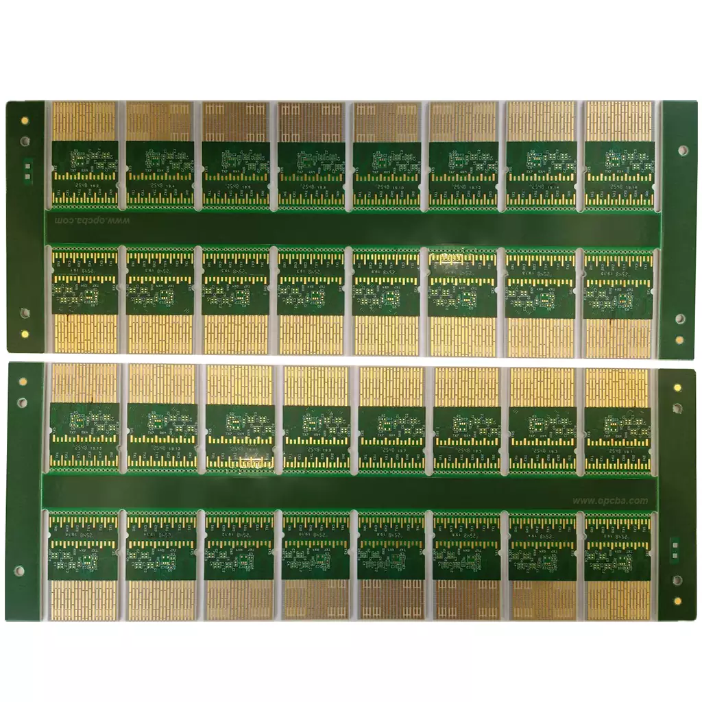
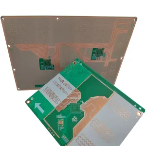
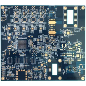
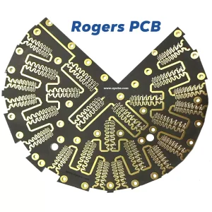
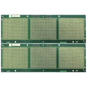
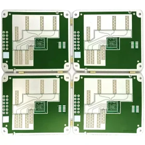
Product overview
A high speed PCB is engineered for fast signal transmission and stable high-frequency operation. Set against a standard board, it holds signal loss, interference and delay far lower, which is the signal integrity modern high-performance electronics depend on.
The board is one branch of printed circuit board technology.
PCB types and manufacturing fundamentals covers the rest of the family. In service, high speed boards carry traffic for 5G, data centers and high-performance computing, where timing has to hold precisely.
Structural composition
Every high speed PCB has a layered structure optimized for high-frequency performance, and each layer carries part of the job of preserving signal quality.
Signal layers carry the high-speed data, and how they are routed is what keeps crosstalk out of the waveform. Between them, dielectric layers set how fast a signal travels and how much of it is lost, so low-loss material is required rather than optional.
Ground and power layers supply stable power and electromagnetic shielding, and they cut noise on high-speed signals at the same time. Copper traces are dimensioned precisely so that impedance matches the target, which is what a reliable link depends on.
Design considerations
Designing a high speed board comes down to a few engineering factors, and each one shows up directly in signal performance and reliability.
Impedance control is not optional. Designers calibrate trace and dielectric properties until they match the target values, which keeps signal reflection out of the channel. Signal integrity then depends on strict layout rules: short traces, no sharp bends, and analog and digital sections kept apart. Those rules are what hold overshoot and jitter down.
Noise reduction relies on solid ground planes and shielding, which block interference from outside the board and from neighboring traces. Thermal management matters as well, since high-speed components generate more heat and dissipating it well is what extends service life.
Material selection
A high speed PCB’s performance depends entirely on its material choices, and every selection is made against the frequencies the design has to pass.
Dielectric substrates use low Dk/Df laminates such as Rogers or Megtron, which cut signal attenuation at ultra-high frequencies. Copper foil is specified low-roughness and high-purity to reduce the skin effect and improve conductivity.
Laminate builds favor multi-layer designs with thick ground and power layers, which improve shielding and resistance to interference. Surface treatments such as ENIG or immersion silver protect the traces underneath and give a surface that solders reliably, with consistent conductivity.
Signal integrity specifications
High-speed performance comes down to controlling loss and impedance together. We build on low-Dk/Df laminates including Rogers RO4000 series, Isola I-Speed and FR408HR, and Panasonic Megtron 6/7, matched to your data rate and budget. Impedance is engineered into the stack-up and verified by coupon testing before shipment; standard ranges are listed on our capability sheet.
| Layers |
4 to 32+ (complex routing builds supported) |
| Minimum trace / space |
3 mil on 18 um base copper |
| Impedance tolerance |
+/-5 ohm below 50 ohm; +/-10% at 50 ohm and above (+/-5% on review) |
| Laser via |
0.10 mm |
| Surface finish |
ENIG, OSP, immersion silver or tin |
Bring the target impedance, reference layers, and dielectric stack to our engineering team, and you get a verified plan with trace geometry back before panel release.
Application areas
High speed boards carry fast, reliable data in industries that cannot tolerate a degraded link, and their signal performance is what separates them from standard boards.
Routers and servers in data centers use them to handle very large volumes of traffic at low latency, which is what cloud computing and big data analysis run on. 5G base stations rely on them for high-frequency, high-bandwidth signals, and those radios carry fast mobile and IoT traffic.
Automotive ADAS uses them for real-time exchange between sensors and the compute module, which driver assistance functions depend on. Consumer electronics use them for fast computing and 4K streaming in premium devices.
Aerospace and medical equipment need the signal to stay stable in extreme environments, whether the hardware flies on a satellite or sits in precision medical gear.
FAQ:
How do you keep insertion loss under control?
Three levers: low-Df laminate selection matched to the data rate, copper foil roughness specified against the loss budget, and impedance held inside the tolerance window from the first panel. Coupon TDR results ship with the lot so you can verify, not trust.
Which laminate grade fits 25G+ per-lane designs?
Panasonic Megtron 6 and Isola I-Speed are the workhorses for 25G+ SERDES runs, with Megtron 7 reserved for the tightest loss budgets. Lower-rate digital sections can ride on less expensive FR-4 in hybrid stacks. Material grading references such as S1000-2 are explained in our guide on what S1000-2 refers to.
What do you need from me to quote an impedance-controlled build?
Three things: target impedances with reference layers, the layer stack-up or a target data rate, and the connector or pin field locations if known. Design-side context on signal paths sits in our article on controlled-impedance trace design.